6©2016 Integrated Device Technology, Inc. Revision D September 27, 2016
83905 Datasheet
AC Electrical Characteristics
Table 6A. AC Characteristics, V
DD
= V
DDO
= 3.3V ± 5%, T
A
= 0°C to 70°C
NOTE: Electrical parameters are guaranteed over the specified ambient operating temperature range, which is established when the
device is mounted in a test socket with maintained transverse airflow greater than 500 lfpm. The device will meet specifications after
thermal equilibrium has been reached under these conditions.
All parameters measured at ƒ f
MAX
using a crystal input unless noted otherwise.
Terminated at 50 to V
DDO
/2.
NOTE 1: XTAL_IN can be overdriven by a single-ended LVCMOS signal. Please refer to Application Information section.
NOTE 2: Defined as skew between outputs at the same supply voltage and with equal load conditions. Measured at V
DDO
/2.
NOTE 3: This parameter is defined in accordance with JEDEC Standard 65.
NOTE 4: See phase noise plot.
NOTE 5: These parameters are guaranteed by characterization. Not tested in production.
Table 6B. AC Characteristics, V
DD
= V
DDO
= 2.5V ± 5%, T
A
= 0°C to 70°C
NOTE: Electrical parameters are guaranteed over the specified ambient operating temperature range, which is established when the
device is mounted in a test socket with maintained transverse airflow greater than 500 lfpm. The device will meet specifications after
thermal equilibrium has been reached under these conditions.
All parameters measured at ƒ f
MAX
using a crystal input unless noted otherwise.
Terminated at 50 to V
DDO
/2.
NOTE 1: XTAL_IN can be overdriven by a single-ended LVCMOS signal. Please refer to Application Information section.
NOTE 2: Defined as skew between outputs at the same supply voltage and with equal load conditions. Measured at V
DDO
/2.
NOTE 3: This parameter is defined in accordance with JEDEC Standard 65.
NOTE 4: See phase noise plot.
NOTE 5: These parameters are guaranteed by characterization. Not tested in production.
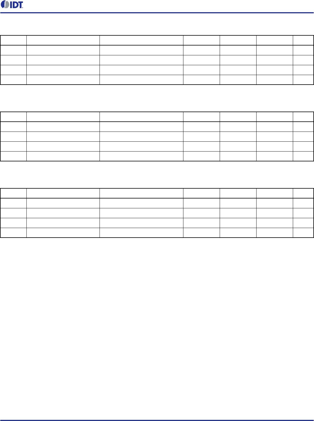
Symbol Parameter Test Conditions Minimum Typical Maximum Units
f
MAX
Output Frequency
Using External Crystal 10 40 MHz
Using External Clock
Source NOTE 1
DC 100 MHz
tsk(o) Output Skew; NOTE 2, 3 80 ps
tjit(Ø) RMS Phase Jitter (Random); NOTE 4
25MHz, Integration Range:
100Hz – 1MHz
0.13 ps
t
R
/ t
F
Output Rise/Fall Time 20% to 80% 200 800 ps
odc Output Duty Cycle 48 52 %
t
EN
Output Enable
Time; NOTE 5
ENABLE1 4 cycles
ENABLE2 4 cycles
t
DIS
Output Disable
Time; NOTE 5
ENABLE1 4 cycles
ENABLE2 4 cycles
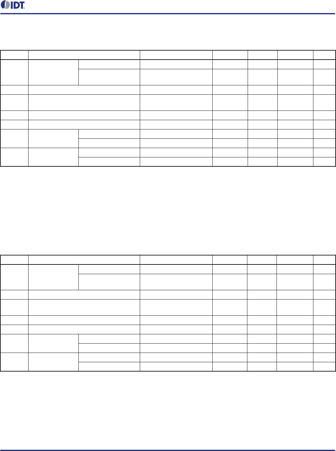
Symbol Parameter Test Conditions Minimum Typical Maximum Units
f
MAX
Output Frequency
Using External Crystal 10 40 MHz
Using External Clock
Source NOTE 1
DC 100 MHz
tsk(o) Output Skew; NOTE 2, 3 80 ps
tjit RMS Phase Jitter (Random); NOTE 4
25MHz, Integration Range:
100Hz – 1MHz
0.26 ps
t
R
/ t
F
Output Rise/Fall Time 20% to 80% 200 800 ps
odc Output Duty Cycle 47 53 %
t
EN
Output Enable
Time; NOTE 5
ENABLE1 4 cycles
ENABLE2 4 cycles
t
DIS
Output Disable
Time; NOTE 5
ENABLE1 4 cycles
ENABLE2 4 cycles