LT3755/LT3755-1/LT3755-2
13
37551fd
applicaTions inForMaTion
zero and full current to achieve a precisely programmed
average current. To make PWM dimming more accurate,
the switch demand current is stored on the VC node dur-
ing the quiescent phase when PWM is low. This feature
minimizes recovery time when the PWM signal goes high.
To further improve the recovery time, a disconnect switch
may be used in the LED current path to prevent the ISP
node from discharging during the PWM signal low phase.
The minimum PWM on or off time is affected by choice
of operating frequency and external component selection.
The data sheet application titled “Buck Mode 500mA LED
Driver for 20kHz PWM Dimming” demonstrates regulated
current pulses as short as 1µs are achievable. The best
overall combination of PWM and analog dimming capabil-
ity is available if the minimum PWM pulse is at least six
switching cycles.
Programming the Switching Frequency
The RT frequency adjust pin allows the user to program
the switching frequency from 100kHz to 1MHz to optimize
efficiency/performance or external component size. Higher
frequency operation yields smaller component size but
increases switching losses and gate driving current, and
may not allow sufficiently high or low duty cycle operation.
Lower frequency operation gives better performance at the
cost of larger external component size. For an appropriate
R
T
resistor value see Table 1. An external resistor from the
RT pin to GND is required—do not leave this pin open.
Table 1. Switching Frequency vs R
T
Value
f
OSC
(kHz) R
T
(kΩ)
1000 10.0
900 11.8
800 13.0
700 15.4
600 17.8
500 21.0
400 26.7
300 35.7
200 53.6
100 100
Duty Cycle Considerations
Switching duty cycle is a key variable defining converter
operation, therefore, its limits must be considered when
programming the switching frequency for a particular
application. The fixed minimum on-time and minimum
off-time (see Figure 4) and the switching frequency define
the minimum and maximum duty cycle of the switch,
respectively. The following equations express the mini-
mum/maximum duty cycle:
Min Duty Cycle = (minimum on-time) switching
frequency
Max Duty Cycle = 1 (minimum off-time) switching
frequency
When calculating the operating limits, the typical values
for on/off-time in the data sheet should be increased by
at least 60ns to allow margin for PWM control latitude,
GATE rise/fall times and SW node rise/fall times.
Figure 4. Typical Minimum On and Off
Pulse Width vs Temperature
Thermal Considerations
The LT3755 is rated to a maximum input voltage of 40V.
Careful attention must be paid to the internal power dis-
sipation of the IC at higher input voltages to ensure that
a junction temperature of 125°C (150°C for H-Grade) is
not exceeded. This junction limit is especially important
LT3755/LT3755-1/LT3755-2
14
37551fd
applicaTions inForMaTion
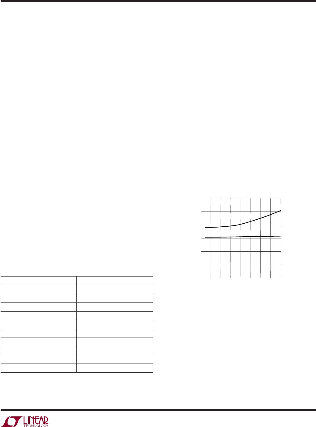
when operating at high ambient temperatures. The ma-
jority of the power dissipation in the IC comes from the
supply current needed to drive the gate capacitance of
the external power MOSFET. This gate drive current can
be calculated as:
I
GATE
= f
SW
• Q
G
A low Q
G
power MOSFET should always be used when op-
erating at high input voltages, and the switching frequency
should also be chosen carefully to ensure that the IC does
not exceed a safe junction temperature. The internal junc-
tion temperature of the IC can be estimated by:
T
J
= T
A
+ [V
IN
(I
Q
+ f
SW
• Q
G
) • θ
JA
]
where T
A
is the ambient temperature, I
Q
is the quiescent
current of the part (maximum 1.7mA) and θ
JA
is the
package thermal impedance (68°C/W for the 3mm × 3mm
QFN package). For example, an application with T
A(MAX)
= 85°C, V
IN(MAX)
= 40V, f
SW
= 400kHz, and having a FET
with Q
G
= 20nC, the maximum IC junction temperature
will be approximately:
T
J
= 85°C + [40V (1.7mA + 400kHz • 20nC) • 68°C/W]
= 111°C
The Exposed Pad on the bottom of the package must be
soldered to a ground plane. This ground should then be
connected to an internal copper ground plane with thermal
vias placed directly under the package to spread out the
heat dissipated by the IC.
If LT3755 junction temperature reaches 165°C, the GATE
and PWMOUT pins will be driven to GND and the soft-
start (SS) pin will be discharged to GND. Switching will
be enabled after device temperature is reduced 10°C. This
function is intended to protect the device during momentary
thermal overload conditions.
Frequency Synchronization (LT3755-1 Only)
The LT3755-1 switching frequency can be synchronized to
an external clock using the SYNC pin. For proper operation,
the R
T
resistor should be chosen for a switching frequency
20% lower than the external clock frequency. The SYNC
pin is disabled during the soft-start period.
Observation of the following guidelines about the SYNC
waveform will ensure proper operation of this feature.
Driving SYNC with a 50% duty cycle waveform is always
a good choice, otherwise, maintain the duty cycle between
20% and 60%. When using both PWM and SYNC features,
the PWM signal rising edge should occur at least 200ns
before the SYNC rising edge (V
IH
) for optimal PWM
performance. If the SYNC pin is not used, it should be
connected to GND.
Open LED Detection (LT3755 and LT3755-2)
The LT3755 and LT3755-2 provide an open-drain status
pin, OPENLED, that pulls low when the FB pin is within
~50mV of its 1.25V regulated voltage. If the open LED
clamp voltage is programmed correctly using the FB pin,
then the FB pin should never exceed 1.1V when LEDs are
connected, therefore, the only way for the FB pin to be within
50mV of the regulation voltage is for an open LED event to
have occurred. The key difference between the LT3755 and
LT3755-2 is the behavior of the OPENLED pin when the FB
pin crosses and re-crosses the FB overvoltage threshold
(1.31V typ). The LT3755-2 asserts/de-asserts OPENLED
freely when crossing the 1.31V threshold. The LT3755,
by comparison, de-asserts OPENLED when FB exceeds
1.31V and is prevented from re-asserting OPENLED until
the FB pin falls below the 1.2V (typ) open LED threshold
and clears the fault. The LT3755-2 has the more general
purpose behavior and is recommended for applications
using OPENLED.
Input Capacitor Selection
The input capacitor supplies the transient input current for
the power inductor of the converter and must be placed
and sized according to the transient current requirements.
The switching frequency, output current and tolerable input
voltage ripple are key inputs to estimating the capacitor
value. An X7R type ceramic capacitor is usually the best
choice since it has the least variation with temperature and
DC bias. Typically, boost and SEPIC converters require a
lower value capacitor than a buck mode converter. As-
suming that a 100mV input voltage ripple is acceptable,
the required capacitor value for a boost converter can be
estimated as follows:
C
IN
(µF) = I
LED
(A)
V
OUT
V
IN
t
SW
(µs)
µF
A µs
LT3755/LT3755-1/LT3755-2
15
37551fd
applicaTions inForMaTion
Therefore, a 10µF capacitor is an appropriate selection
for a 400kHz boost regulator with 12V input, 48V output
and 1A load.
With the same V
IN
voltage ripple of 100mV, the input capaci-
tor for a buck converter can be estimated as follows:
C
IN
(µF) = I
LED
(A) t
SW
(µs) 4.7
µF
A µs
A 10µF input capacitor is an appropriate selection for a
400kHz buck mode converter with a 1A load.
In the buck mode configuration, the input capacitor has
large pulsed currents due to the current returned through
the Schottky diode when the switch is off. In this buck
converter case it is important to place the capacitor as close
as possible to the Schottky diode and to the GND return
of the switch (i.e., the sense resistor). It is also important
to consider the ripple current rating of the capacitor. For
best reliability, this capacitor should have low ESR and
ESL and have an adequate ripple current rating. The RMS
input current for a buck mode LED driver is:
I
IN(RMS)
= I
LED
1 D
( )
D
where D is the switch duty cycle.
Table 2. Recommended Ceramic Capacitor Manufacturers
MANUFACTURER WEB
TDK www.tdk.com
Kemet www.kemet.com
Murata www.murata.com
Taiyo Yuden www.t-yuden.com
Output Capacitor Selection
The selection of the output capacitor depends on the load
and converter configuration, i.e., step-up or step-down
and the operating frequency. For LED applications, the
equivalent resistance of the LED is typically low and the
output filter capacitor should be sized to attenuate the
current ripple. Use of X7R type ceramic capacitors is
recommended.
To achieve the same LED ripple current, the required filter
capacitor is larger in the boost and buck-boost mode ap-
plications than that in the buck mode applications. Lower
operating frequencies will require proportionately higher
capacitor values.
Soft-Start Capacitor Selection
For many applications, it is important to minimize the
inrush current at start-up. The built-in soft-start circuit
significantly reduces the start-up current spike and output
voltage overshoot. The soft-start interval is set by the soft-
start capacitor selection according to the equation:
T
SS
= C
SS
2V
10µA
A typical value for the soft-start capacitor is 0.01µF. The
soft-start pin reduces the oscillator frequency and the
maximum current in the switch. The soft-start capacitor
is discharged when SHDN/UVLO falls below its threshold,
during an overtemperature event or during an INTV
CC
undervoltage event. During start-up with SHDN/UVLO,
charging of the soft-start capacitor is enabled after the
first PWM high period.
Power MOSFET Selection
For applications operating at high input or output voltages,
the power NMOS FET switch is typically chosen for drain
voltage V
DS
rating and low gate charge Q
G
. Consideration
of switch on-resistance, R
DS(ON)
, is usually secondary be-
cause switching losses dominate power loss. The INTV
CC
regulator on the LT3755 has a fixed current limit to protect
the IC from excessive power dissipation at high V
IN
, so the
FET should be chosen so that the product of Q
G
at 7V and
switching frequency does not exceed the INTV
CC
current
limit. For driving LEDs be careful to choose a switch with
a V
DS
rating that exceeds the threshold set by the FB pin
in case of an open-load fault. Several MOSFET vendors
are listed in Table 3. The MOSFETs used in the application
circuits in this data sheet have been found to work well
with the LT3755. Consult factory applications for other
recommended MOSFETs.
Table 3. MOSFET Manufacturers
VENDOR WEB
Vishay Siliconix www.vishay.com
Fairchild www.fairchildsemi.com
International Rectifier www.irf.com

LT3755IMSE-2#TRPBF

Mfr. #:
Manufacturer:
Analog Devices / Linear Technology
Description:
LED Lighting Drivers 75V Full-Featured LED Controller
Lifecycle:
New from this manufacturer.
Delivery:
DHL FedEx Ups TNT EMS
Payment:
T/T Paypal Visa MoneyGram Western Union