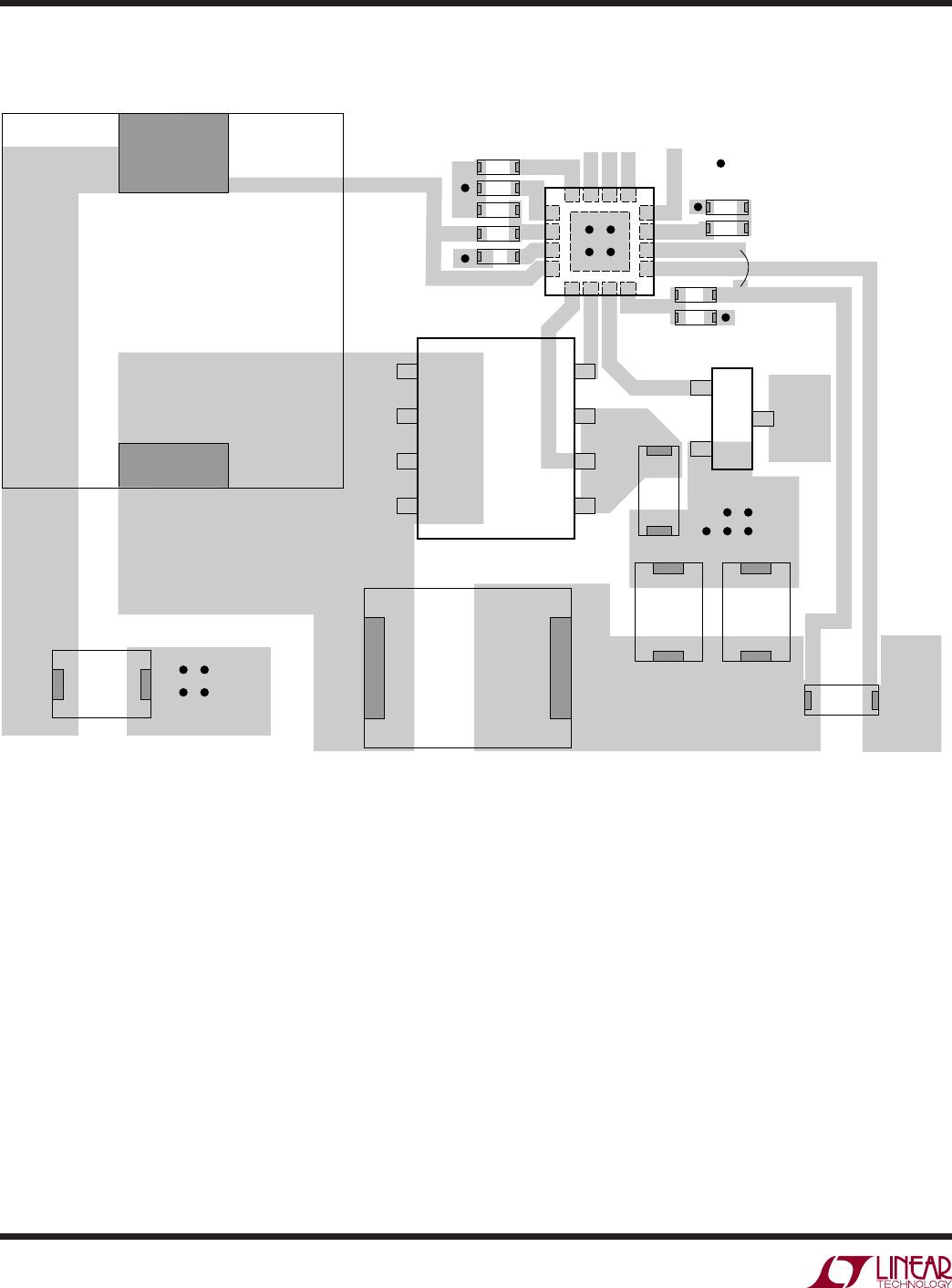
LT3755/LT3755-1/LT3755-2
16
37551fd
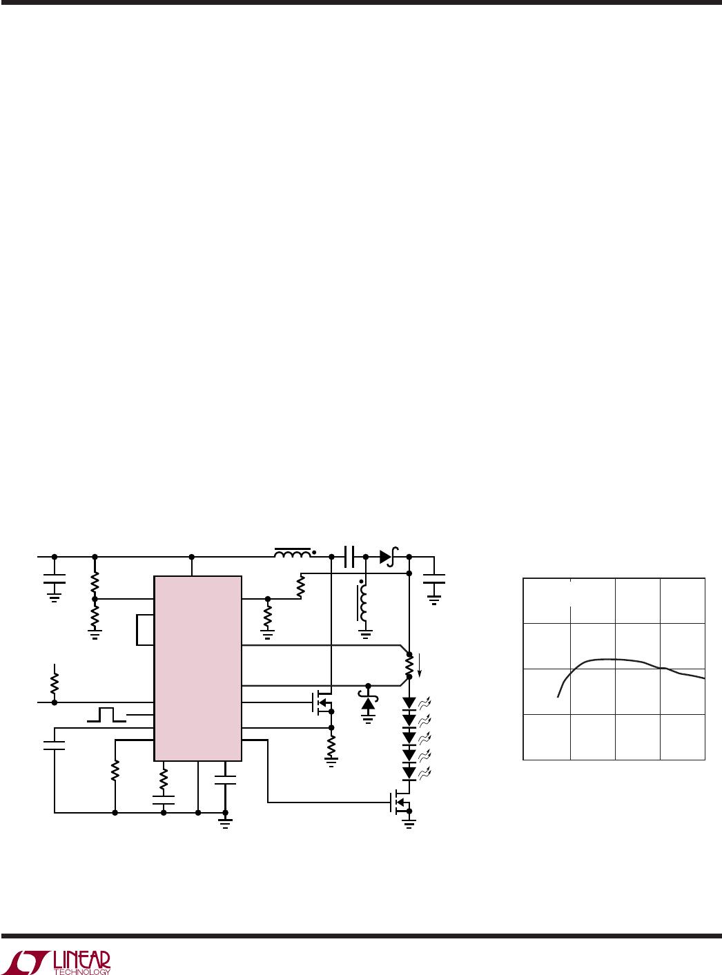
applicaTions inForMaTion
Schottky Rectifier Selection
The power Schottky diode conducts current during the
interval when the switch is turned off. Select a diode rated
for the maximum SW voltage. If using the PWM feature for
dimming, it is important to consider diode leakage, which
increases with the temperature, from the output during the
PWM low interval. Therefore, choose the Schottky diode
with sufficiently low leakage current. Table 4 has some
recommended component vendors.
Table 4. Schottky Rectifier Manufacturers
VENDOR WEB
On Semiconductor www.onsemi.com
Diodes, Inc. www.diodes.com
Central Semiconductor www.centralsemi.com
Sense Resistor Selection
The resistor, R
SENSE
, between the source of the exter-
nal NMOS FET and GND should be selected to provide
adequate switch current to drive the application without
exceeding the 108mV (typical) current limit threshold on
the SENSE pin of LT3755. For buck mode applications,
select a resistor that gives a switch current at least 30%
greater than the required LED current. For buck mode,
select a resistor according to:
R
SENSE,BUCK
≤
0.07V
I
LED
For buck-boost, select a resistor according to:
R
SENSE,BUCK-BOOST
≤
V
IN
• 0.07V
V
IN
+ V
LED
( )
I
LED
For boost, select a resistor according to:
R
SENSE,BOOST
≤
V
IN
• 0.07V
V
LED
• I
LED
These equations provide an estimate of the sense resistor
value based on reasonable assumptions about induc-
tor current ripple during steady state switching. Lower
values of sense resistor may be required in applications
where inductor ripple current is higher. Examples include
applications with current limited operation at high duty
cycle, and those with discontinuous conduction mode
(DCM) switching. It is always prudent to verify the peak
inductor current in the application to ensure the sense
resistor selection provides margin to the SENSE current
limit threshold.
The placement of R
SENSE
should be close to the source of
the NMOS FET and GND of the LT3755. The SENSE input
to LT3755 should be a Kelvin connection to the positive
terminal of R
SENSE
.
Inductor Selection
The inductor used with the LT3755 should have a saturation
current rating appropriate to the maximum switch current
selected with the R
SENSE
resistor. Choose an inductor value
based on operating frequency, input and output voltage to
provide a current mode ramp on SENSE during the switch
on-time of approximately 20mV magnitude. The following
equations are useful to estimate the inductor value for
continuous conduction mode operation:
L
BUCK
=
R
SENSE
• V
LED
V
IN
– V
LED
( )
V
IN
• 0.02V • f
OSC
L
BUCK-BOOST
=
R
SENSE
• V
LED
• V
IN
V
LED
+ V
IN
( )
• 0.02V • f
OSC
L
BOOST
=
R
SENSE
• V
IN
V
LED
– V
IN
( )
V
LED
• 0.02V • f
OSC
Table 5 provides some recommended inductor vendors.
Table 5. Inductor Manufacturers
VENDOR WEB
Sumida www.sumida.com
Würth Elektronik www.we-online.com
Coiltronics www.cooperet.com
Vishay www.vishay.com
Coilcraft www.coilcraft.com
Loop Compensation
The LT3755 uses an internal transconductance error ampli-
fier whose VC output compensates the control loop. The
external inductor, output capacitor and the compensation
resistor and capacitor determine the loop stability.