©2011 Silicon Storage Technology, Inc. DS25028A 08/11
2
16 Mbit / 32 Mbit Multi-Purpose Flash Plus
SST39VF1601 / SST39VF3201
SST39VF1602 / SST39VF3202
Not Recommended for New Designs
Microchip Technology Company
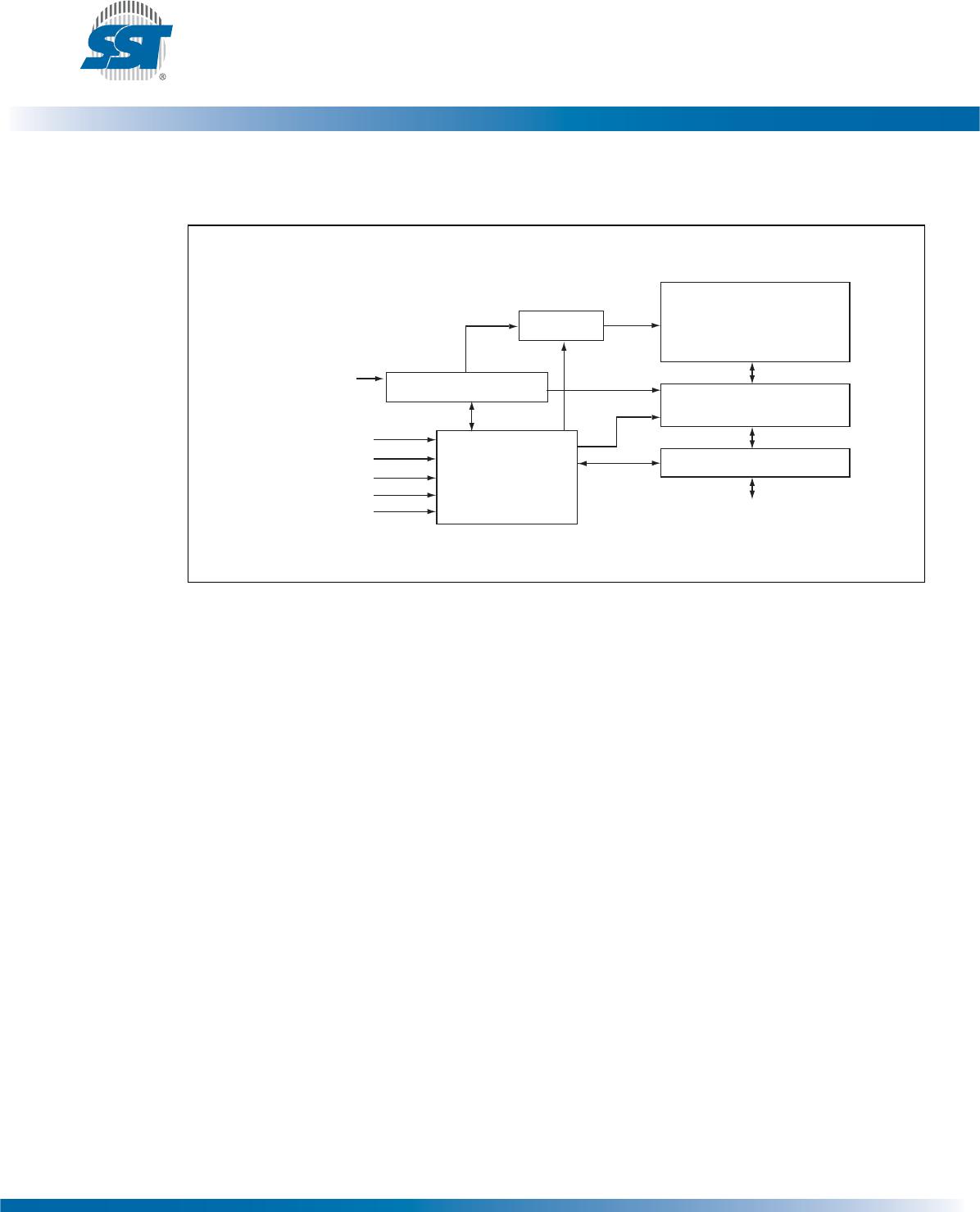
Product Description
The SST39VF160x and SST39VF320x devices are 1M x16 and 2M x16, respectively, CMOS Multi-
Purpose Flash Plus (MPF+) manufactured with SST’s proprietary, high performance CMOS Super-
Flash technology. The split-gate cell design and thick-oxide tunneling injector attain better reliability
and manufacturability compared with alternate approaches. The SST39VF160x/320x write (Program
or Erase) with a 2.7-3.6V power supply. These devices conform to JEDEC standard pinouts for x16
memories.
Featuring high performance Word-Program, the SST39VF160x/320x devices provide a typical Word-
Program time of 7 µsec. These devices use Toggle Bit or Data# Polling to indicate the completion of
Program operation. To protect against inadvertent write, they have on-chip hardware and Software
Data Protection schemes. Designed, manufactured, and tested for a wide spectrum of applications,
these devices are offered with a guaranteed typical endurance of 100,000 cycles. Data retention is
rated at greater than 100 years.
The SST39VF160x/320x devices are suited for applications that require convenient and economical
updating of program, configuration, or data memory. For all system applications, they significantly
improve performance and reliability, while lowering power consumption. They inherently use less
energy during Erase and Program than alternative flash technologies. The total energy consumed is a
function of the applied voltage, current, and time of application. Since for any given voltage range, the
SuperFlash technology uses less current to program and has a shorter erase time, the total energy
consumed during any Erase or Program operation is less than alternative flash technologies. These
devices also improve flexibility while lowering the cost for program, data, and configuration storage
applications.
The SuperFlash technology provides fixed Erase and Program times, independent of the number of
Erase/Program cycles that have occurred. Therefore the system software or hardware does not have
to be modified or de-rated as is necessary with alternative flash technologies, whose Erase and Pro-
gram times increase with accumulated Erase/Program cycles.
To meet high density, surface mount requirements, the SST39VF160x/320x are offered in 48-lead
TSOP and 48-ball TFBGA packages. See Figures 2 and 3 for pin assignments.