REV. 0
Information furnished by Analog Devices is believed to be accurate and
reliable. However, no responsibility is assumed by Analog Devices for its
use, nor for any infringements of patents or other rights of third parties
which may result from its use. No license is granted by implication or
otherwise under any patent or patent rights of Analog Devices.
a
AD9841A/AD9842A
One Technology Way, P.O. Box 9106, Norwood, MA 02062-9106, U.S.A.
Tel: 781/329-4700 World Wide Web Site: http://www.analog.com
Fax: 781/326-8703 © Analog Devices, Inc., 2001
Complete 20 MSPS
CCD Signal Processors
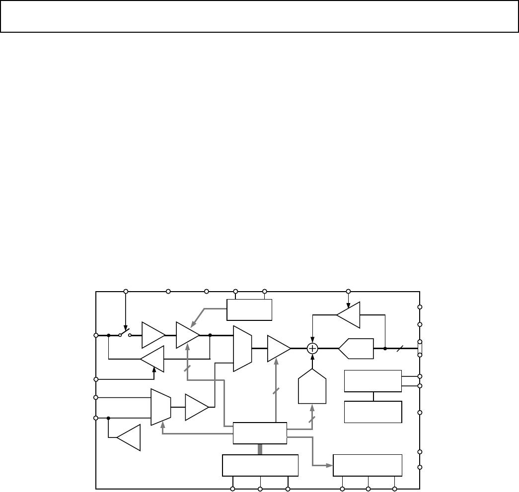
FUNCTIONAL BLOCK DIAGRAM
DATACLKSHDSHP
BANDGAP
REFERENCE
2:1
MUX
DOUT
AUX2IN
CLPDM
CCDIN
OFFSET
DAC
PBLK
AUX1IN
VRT
VRB
INTERNAL
TIMING
INTERNAL
BIAS
2dB–36dB
AVDD
DVDD
DVSS
AVSS
DRVDD
DRVSS
10
8
CML
DIGITAL
INTERFACE
SDATASCK
SL
CLPOB
10/12
CDS
VGA
CLP
BUF
2:1
MUX
CLP
AD9841A/AD9842A
CONTROL
REGISTERS
CLP
ADC
4dB 6dB
COLOR
STEERING
HD VD
PxGA
6
FEATURES
20 MSPS Correlated Double Sampler (CDS)
4 dB 6 dB 6-Bit Pixel Gain Amplifier (
PxGA
®
)
2 dB to 36 dB 10-Bit Variable Gain Amplifier (VGA)
Low Noise Clamp Circuits
Analog Preblanking Function
10-Bit (9841) or 12-Bit (9842) 20 MSPS A/D Converter
Auxiliary Inputs with VGA and Input Clamp
3-Wire Serial Digital Interface
3 V Single Supply Operation
Low Power: 65 mW @ 2.7 V Supply
48-Lead LQFP Package
APPLICATIONS
Digital Still Cameras
Digital Video Camcorders
PRODUCT DESCRIPTION
The AD9841A and AD9842A are complete analog signal proces-
sors for CCD applications. Both products feature a 20 MHz
single-channel architecture designed to sample and condition
the outputs of interlaced and progressive scan area CCD arrays.
The AD9841A/AD9842A’s signal chain consists of an input
clamp, correlated double sampler (CDS), Pixel Gain Amplifier
(PxGA), digitally controlled variable gain amplifier (VGA),
black level clamp, and A/D converter. The AD9841A offers 10-bit
ADC resolution, while the AD9842A contains a true 12-bit
ADC. Additional input modes are provided for processing analog
video signals.
The internal registers are programmed through a 3-wire serial
digital interface. Programmable features include gain adjustment,
black level adjustment, input configuration, and power-down modes.
The AD9841A and AD9842A operate from a single 3 V power
supply, typically dissipate 78 mW, and are packaged in a 48-
lead LQFP.
PxGA is a registered trademark of Analog Devices, Inc.
REV. 0
–2–
AD9841A/AD9842A–SPECIFICATIONS
GENERAL SPECIFICATIONS
Parameter Min Typ Max Unit
TEMPERATURE RANGE
Operating –20 +85 °C
Storage –65 +150 °C
POWER SUPPLY VOLTAGE
Analog, Digital, Digital Driver 2.7 3.6 V
POWER CONSUMPTION
Normal Operation (Specified Under Each Mode of Operation)
Power-Down Modes
Fast Recovery Mode 30 mW
Standby 5 mW
Total Power-Down 1 mW
MAXIMUM CLOCK RATE 20 MHz
A/D CONVERTER (AD9841A)
Resolution 10 Bits
Differential Nonlinearity (DNL) ± 0.4 ± 1.0 LSB
No Missing Codes 10 Bits Guaranteed
Full-Scale Input Voltage 2.0 V
Data Output Coding Straight Binary
A/D CONVERTER (AD9842A)
Resolution 12 Bits
Differential Nonlinearity (DNL) ± 0.5 ± 1.0 LSB
No Missing Codes 12 Bits Guaranteed
Full-Scale Input Voltage 2.0 V
Data Output Coding Straight Binary
VOLTAGE REFERENCE
Reference Top Voltage (VRT) 2.0 V
Reference Bottom Voltage (VRB) 1.0 V
Specifications subject to change without notice.
DIGITAL SPECIFICATIONS
Parameter Symbol Min Typ Max Unit
LOGIC INPUTS
High Level Input Voltage V
IH
2.1 V
Low Level Input Voltage V
IL
0.6 V
High Level Input Current I
IH
10 µA
Low Level Input Current I
IL
10 µA
Input Capacitance C
IN
10 pF
LOGIC OUTPUTS
High Level Output Voltage, I
OH
= 2 mA V
OH
2.2 V
Low Level Output Voltage, I
OL
= 2 mA V
OL
0.5 V
Specifications subject to change without notice.
(DRVDD = 2.7 V, C
L
= 20 pF unless otherwise noted.)
(T
MIN
to T
MAX
, AVDD = DVDD = 3.0 V, f
DATACLK
= 20 MHz, unless otherwise noted.)
REV. 0
–3–
AD9841A/AD9842A
Parameter Min Typ Max Unit Notes
P
OWER CONSUMPTION 78 mW See TPC 1 for Power Curves
MAXIMUM CLOCK RATE 20 MHz
CDS
Gain 0 dB
Allowable CCD Reset Transient
1
500 mV See Input Waveform in Footnote 1
Max Input Range Before Saturation
1
1.0 V p-p PxGA
Gain at 4 dB
Max CCD Black Pixel Amplitude
1
200 mV
PIXEL GAIN AMPLIFIER (PxGA)
Max Input Range 1.0 V p-p PxGA
Gain at 4 dB
Max Output Range 1.6 V p-p At Any PxGA
Gain
Gain Control Resolution 64 Steps
Gain Monotonicity Guaranteed
Gain Range (Two’s Complement Coding) See Figure 28 for PxGA
Gain Curve
Min Gain (PxGA Gain Code 32) –2 dB
Max Gain (PxGA Gain Code 31) 10 dB
VARIABLE GAIN AMPLIFIER (VGA)
Max Input Range 1.6 V p-p
Max Output Range 2.0 V p-p
Gain Control Resolution 1024 Steps
Gain Monotonicity . Guaranteed
Gain Range See Figure 29 for VGA Gain Curve
Low Gain (VGA Gain Code 91) 2 dB
Max Gain (VGA Gain Code 1023) 36 dB
BLACK LEVEL CLAMP
Clamp Level Resolution 256 Steps
Clamp Level Measured at ADC Output
Min Clamp Level 0 LSB
Max Clamp Level 63.75 LSB
SYSTEM PERFORMANCE Specifications Include Entire Signal Chain
Gain Accuracy, VGA Code 91 to 1023
2
–0.5 +0.5 Use Equations on Page 19 to Calculate Gain
PxGA
Gain Accuracy
Min Gain (PxGA
Register Code 32) –1 0 +1 dB VGA Gain Fixed at 2 dB (Code 91)
Max Gain (PxGA
Code 31) 11 12 13 dB VGA Gain Fixed at 2 dB (Code 91)
Peak Nonlinearity, 500 mV Input Signal 0.1 % 12 dB Gain Applied
Peak Nonlinearity, 800 mV Input Signal 0.4 % 8 dB Gain Applied
Total Output Noise 0.2 LSB rms AC Grounded Input, 6 dB Gain Applied
Power Supply Rejection (PSR) 40 dB Measured with Step Change on Supply
POWER-UP RECOVERY TIME Normal Clock Signals Applied
Fast Recovery Mode 0.1 ms
Reference Standby Mode 1 ms
Total Shutdown Mode 3 ms
Power-Off Condition 15 ms
NOTES
1
Input Signal Characteristics defined as follows:
200mV MAX
OPTICAL BLACK PIXEL
500mV TYP
RESET TRANSIENT
1V MAX
INPUT SIGNAL RANGE
2
PxGA gain fixed at 4 dB.
Specifications subject to change without notice.
AD9841A CCD-MODE SPECIFICATIONS
(T
MIN
to T
MAX
, AVDD = DVDD = 3.0 V, f
DATACLK
= f
SHP
= f
SHD
= 20 MHz, unless other-
wise noted.)
AD9841AJSTZRL

Mfr. #:
Manufacturer:
Analog Devices Inc.
Description:
Analog Front End - AFE 10-Bit 20MHz CCD Signal Processor
Lifecycle:
New from this manufacturer.
Delivery:
DHL FedEx Ups TNT EMS
Payment:
T/T Paypal Visa MoneyGram Western Union

Products related to this Datasheet