AD7414/AD7415
Rev. F | Page 12 of 20
SERIAL INTERFACE
Control of the AD7414/AD7415 is carried out via the I
2
C-
compatible serial bus. The AD7414/AD7415 are connected to
this bus as slave device, under the control of a master device,
such as the processor.
SERIAL BUS ADDRESS
Like all I
2
C-compatible devices, the AD7414/AD7415 have a
7-bit serial address. The four MSBs of this address for the
AD7414/AD7415 are set to 1001. The AD7414/AD7415 are
available in four versions: AD7414/AD7415-0, AD7414/
AD7415-1, AD7414-2, and AD7414-3. The first two versions
have three different I
2
C addresses available, which are selected
by either tying the AS pin to GND, to V
DD
, or letting the pin
float (see Table 4 ). By giving different addresses for the four
versions, up to eight AD7414s or six AD7415s can be connected
to a single serial bus, or the addresses can be set to avoid
conflicts with other devices on the bus.
The serial bus protocol operates as follows.
The master initiates data transfer by establishing a START
condition, defined as a high-to-low transition on the serial data
line SDA, while the serial clock line SCL remains high. This
indicates that an address/data stream follows. All slave periph-
erals connected to the serial bus respond to the START condi-
tion and shift in the next eight bits, consisting of a 7-bit address
(MSB first) plus an R/
W
bit, which determines the direction of
the data transfer and whether data is written to or read from the
slave device.
The peripheral whose address corresponds to the transmitted
address responds by pulling the data line low during the low
period before the ninth clock pulse, known as the acknowledge
bit. All other devices on the bus remain idle while the selected
device waits for data to be read from or written to it. If the R/
W
bit is 0, the master writes to the slave device. If the R/
W
bit is 1,
the master reads from the slave device.
Data is sent over the serial bus in sequences of nine clock
pulses, eight bits of data followed by an acknowledge bit from
the receiver of data. Transitions on the data line must occur
during the low period of the clock signal and remain stable
during the high period, because a low-to-high transition when
the clock is high may be interpreted as a STOP signal.
When all data bytes have been read or written, stop conditions
are established. In WRITE mode, the master pulls the data line
high during the 10th clock pulse to assert a STOP condition. In
READ mode, the master device pulls the data line high during
the low period before the ninth clock pulse. This is known as
No Acknowledge. The master then takes the data line low
during the low period before the 10th clock pulse, then high
during the 10th clock pulse to assert a STOP condition.
Any number of bytes of data may be transferred over the serial
bus in one operation, but it is not possible to mix read and write
in one operation. The type of operation is determined at the
beginning and cannot then be changed without starting a new
operation.
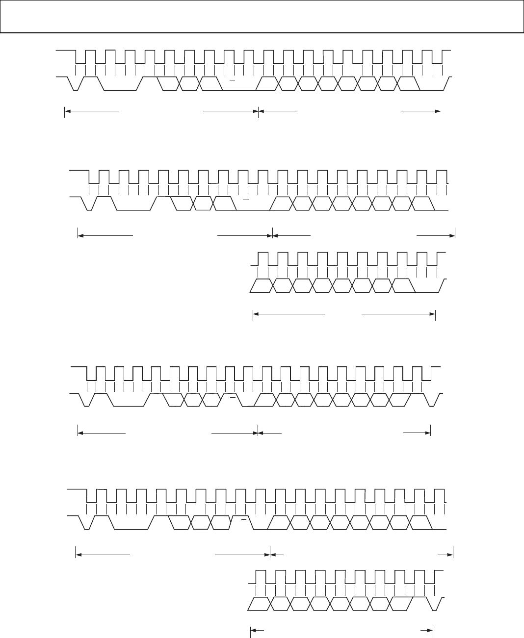
WRITE MODE
Depending on the register being written to, there are two
different writes for the AD7414/AD7415.
Writing to the Address Pointer Register for a Subsequent
Read
In order to read data from a particular register, the address
pointer register must contain the address of that register. If it
does not, the correct address must be written to the address
pointer register by performing a single-byte write operation, as
shown in Figure 10. The write operation consists of the serial
bus address followed by the address pointer byte. No data is
written to any of the data registers. A read operation is then
performed to read the register.
Writing a Single Byte of Data to the Configuration
Register,T
HIGH
Register, or T
LOW
Register
All three registers are 8-bit registers, so only one byte of data
can be written to each register. Writing a single byte of data to
one of these registers consists of the serial bus address, the data
register address written to the address pointer register, followed
by the data byte written to the selected data register. This is
illustrated in Figure 11.
READ MODE
Reading data from the AD7414/AD7415 is a 1- or 2-byte
operation. Reading back the contents of the configuration
register, the T
HIGH
register, or the T
LOW
register is a single-byte
read operation, as shown in Figure 12. The register address was
previously set up by a single-byte write operation to the address
pointer register. Once the register address has been set up, any
number of reads can subsequently be performed from that
register without having to write to the address pointer register
again. To read from another register, the address pointer
register has to be written to again to set up the relevant register
address.
Reading data from the temperature value register is a 2-byte
operation, as shown in Figure 13. The same rules apply for a
2-byte read as a 1-byte read.