AD7414/AD7415
Rev. F | Page 13 of 20
SMBUS ALERT
The AD7414 ALERT output is an SMBus interrupt line for
devices that want to trade their ability to master for an extra
pin. The AD7414 is a slave-only device and uses the SMBus
ALERT to signal to the host device that it wants to talk. The
SMBus ALERT on the AD7414 is used as an overtemperature
indicator.
The ALERT pin has an open-drain configuration that allows the
ALERT outputs of several AD7414s to be wire-AND’ed together
when the ALERT pin is active low. Use D4 of the configuration
register to set the active polarity of the ALERT output. The
power-up default is active low. The ALERT function can be
disabled or enabled by setting D5 of the configuration register
to 1 or 0, respectively.
The host device can process the ALERT interrupt and
simultaneously access all SMBus ALERT devices through the
alert response address. Only the device that pulled the ALERT
low acknowledges the Alert Response Address (ARA). If more
than one device pulls the ALERT pin low, the highest priority
(lowest address) device wins communication rights via standard
I
2
C arbitration during the slave address transfer.
The ALERT output becomes active when the value in the
temperature value register exceeds the value in the T
HIGH
register. It is reset when a write operation to the configuration
register sets D3 to 1 or when the temperature falls below the
value stored in the T
LOW
register.
The ALERT output requires an external pull-up resistor. This
can be connected to a voltage different from V
DD
, provided the
maximum voltage rating of the ALERT output pin is not
exceeded. The value of the pull-up resistor depends on the
application, but it should be as large as possible to avoid
excessive sink currents at the ALERT output, which can heat the
chip and affect the temperature reading.
POWER-ON DEFAULTS
The AD7414/AD7415 always power up with these defaults:
Address pointer register pointing to the temperature value
register.
T
HIGH
register loaded with 7Fh.
T
LOW
register loaded with 80h.
Configuration register loaded with 40h.
Note that the AD7415 does not have any T
HIGH
or T
LOW
registers.
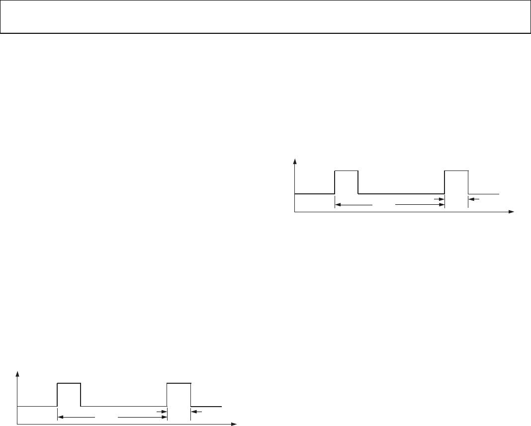
OPERATING MODES
Mode 1
This is the power-on default mode of the AD7414/AD7415. In
this mode, the AD7414/AD7415 does a temperature conversion
every 800 ms and then partially powers down until the next
conversion occurs.
If a one-shot operation (setting D2 of the configuration register
to a 1) is performed between automatic conversions, a conver-
sion is initiated right after the write operation. After this
conversion, the part returns to performing a conversion every
800 ms.
Depending on where a serial port access occurs during a
conversion, that conversion might be aborted. If the conversion
is completed before the part recognizes a serial port access, the
temperature register is updated with the new conversion. If the
conversion is completed after the part recognizes a serial port
access, the internal logic prevents the temperature register from
being updated, because corrupt data could be read.
A temperature conversion can start anytime during a serial port
access (other than a one-shot operation), but the result of that
conversion is loaded into the temperature register only if the
serial port access is not active at the end of the conversion.
Mode 2
The only other mode in which the AD7414/AD7415 operates is
the full power-down mode. This mode is usually used when
temperature measurements are required at a very slow rate. The
power consumption of the part can be greatly reduced in this
mode by writing to the part to go to a full power-down. Full
power-down is initiated right after D7 of the configuration
register is set to 1.
When a temperature measurement is required, a write
operation can be performed to power up the part and put it into
one-shot mode (setting D2 of the configuration register to a 1).
The power-up takes approximately 4 μs. The part then performs
a conversion and is returned to full power-down. The
temperature value can be read in the full power-down mode,
because the serial interface is still powered up.