AD7414/AD7415
Rev. F | Page 4 of 20
Parameter A Version Unit Test Conditions/Comments
AC ELECTRICAL CHARACTERISTICS
8, 9
Serial Clock Period, t
1
2.5 μs min See Figure 2
Data In Setup Time to SCL High, t
2
50 ns min See Figure 2
Data Out Stable after SCL Low, t
3
0 ns min See Figure 2
SDA Low Setup Time to SCL Low
(Start Condition), t
4
50 ns min See Figure 2
SDA High Hold Time after SCL High
(Stop Condition), t
5
50 ns min See Figure 2
SDA and SCL Fall Time, t
6
90 ns max See Figure 2
Data Hold Time, t
7
35 ns min See Figure 2
Power-Up Time 4 μs typ
1
Accuracy specifications apply only to voltages listed under Test Conditions. See Temperature Accuracy vs. Supply section for typical accuracy performance over the
full V
DD
supply range.
2
100% production tested at 40°C to these limits.
3
These current values can be used to determine average power consumption at different one-shot conversion rates. Average power consumption at the automatic
conversion rate of 1.25 kHz is 940 μW.
4
This peak supply current is required for 29 μs (the conversion time plus power-up time) out of every 800 μs (the conversion rate).
5
These current values are derived by not issuing a stop condition at the end of a write or read, thus preventing the part from going into a conversion.
6
The current is derived assuming a 400 kHz serial clock being active continuously.
7
On power-up, the initial input current, I
IN
, on the AS pin is typically 50 μA.
8
The SDA and SCL timing is measured with the input filters turned on so as to meet the fast mode I
2
C specification. Switching off the input filters improves the transfer
rate but has a negative effect on the EMC behavior of the part.
9
Guaranteed by design. Not tested in production.
SCL
SDA
DATA IN
SDA
DATA OUT
t
1
t
2
t
7
t
3
t
4
t
5
t
6
02463-002
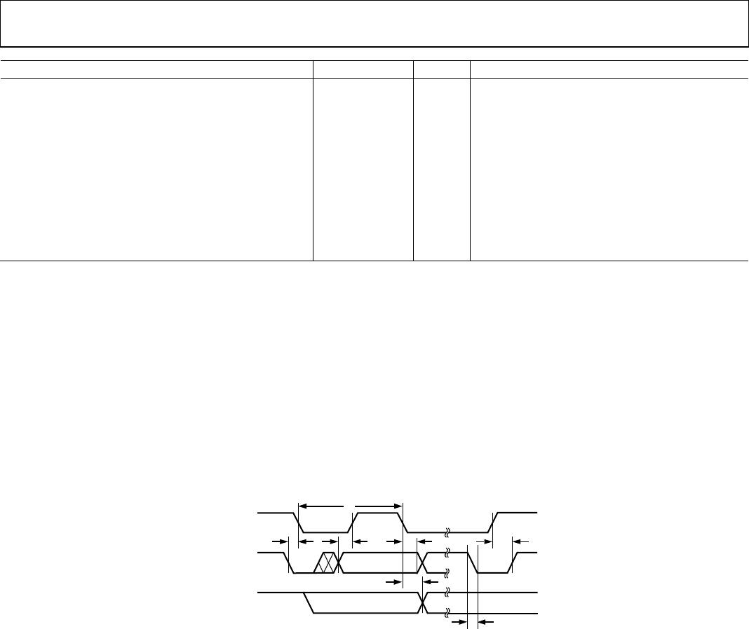
Figure 2. Diagram for Serial Bus Timing
AD7414/AD7415
Rev. F | Page 5 of 20
ABSOLUTE MAXIMUM RATINGS
Table 2.
Parameter Rating
V
DD
to GND −0.3 V to +7 V
SDA Input Voltage to GND −0.3 V to +7 V
SDA Output Voltage to GND −0.3 V to +7 V
SCL Input Voltage to GND −0.3 V to +7 V
ALERT Output Voltage to GND −0.3 V to +7 V
Operating Temperature Range −40°C to +125°C
Storage Temperature Range −65°C to +150°C
Junction Temperature 150°C
5-Lead SOT-23 (RJ-5)
Power Dissipation
1, 2
W
MAX
= (T
JMAX
− T
A
)/θ
JA
Thermal Impedance
3
θ
JA
, Junction-to-Ambient (still air) 240°C/W
6-Lead SOT-23 (RJ-6)
Power Dissipation
1, 2
W
MAX
= (T
JMAX
− T
A
)/θ
JA
Thermal Impedance
3
θ
JA
, Junction-to-Ambient (still air) 190.4°C/W
8-Lead MSOP (RM-8)
Power Dissipation
1, 2
W
MAX
= (T
JMAX
− T
A
)/θ
JA
Thermal Impedance
3
θ
JA
, Junction-to-Ambient (still air) 205.9°C/W
θ
JC
, Junction-to-Case 43.74°C/W
IR Reflow Soldering
Peak Temperature 220°C (0°C/5°C)
Time at Peak Temperature 10 sec to 20 sec
Ramp-up Rate 3°C/s max
Ramp-down Rate
6°C/s max
Ramp from 25°C to Peak Temperature 6 minutes max
IR Reflow Soldering in Pb-Free Package
Peak Temperature 260°C (0°C)
Time at Peak Temperature 20 sec to 40 sec
Ramp Rate 3°C/s max
Ramp-Down Rate
6°C/s max
Ramp from 25°C to Peak Temperature 8 minutes max
1
Values relate to package being used on a standard 2-layer PCB.
2
T
A
= ambient temperature.
3
Junction-to-case resistance is applicable to components featuring a
preferential flow direction, such as components mounted on a heat sink.
Junction-to-ambient resistance is more useful for air-cooled, PCB-mounted
components.
Stresses above those listed under Absolute Maximum Ratings
may cause permanent damage to the device. This is a stress
rating only; functional operation of the device at these or any
other conditions above those indicated in the operational
section of this specification is not implied. Exposure to absolute
maximum rating conditions for extended periods may affect
device reliability.
ESD CAUTION
AD7414/AD7415
Rev. F | Page 6 of 20
PIN CONFIGURATIONS AND FUNCTION DESCRIPTIONS
AS
SDA
1
6
V
DD
SCL
GND 2
5
ALERT
3
4
AD7414
Top View
(Not to Scale)
02463-003
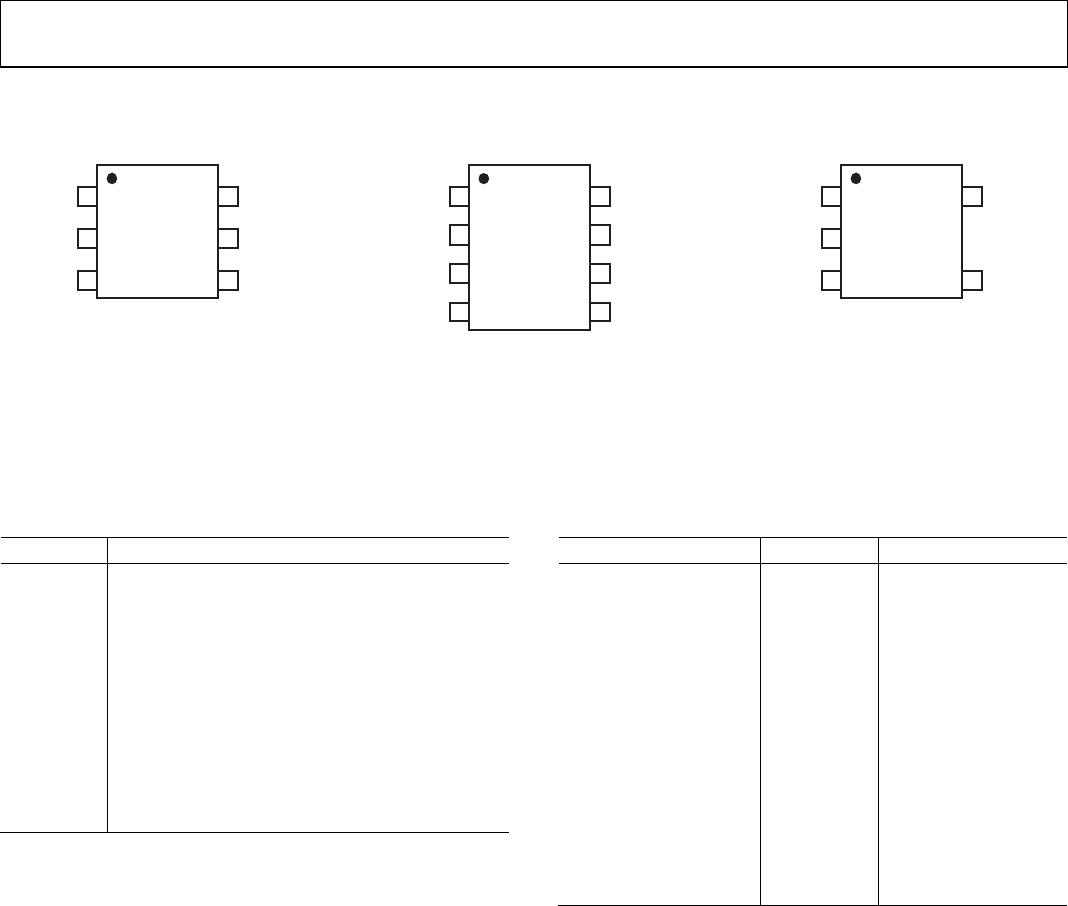
Figure 3. AD7414 Pin Configuration (SOT-23)
02463-004
SCL V
DD
NC
NC
A
LER
T
GND
SDA 2
7
AS
NC = NO CONNECT
1
8
3
6
4
5
AD7414
Top View
(Not to Scale)
Figure 4. AD7414 Pin Configuration (MSOP)
AS
SDA
1
5
V
DD
SCL
GND 2
3
4
AD7415
Top View
(Not to Scale)
02463-005
Figure 5. AD7415 Pin Configuration (SOT-23)
Table 3. Pin Function Descriptions
Mnemonic Description
AS
Logic Input. Address select input that selects one
of three I
2
C addresses for the AD7414/AD7415 (see
Table 4). Recommend a pull-up or pull-down
resistor of 1 kΩ.
GND Analog and Digital Ground.
V
DD
Positive Supply Voltage, 2.7 V to 5.5 V.
SDA
Digital I/O. Serial bus bidirectional data. Open-
drain output.
ALERT
AD7414 Digital Output. Overtemperature
indicator becomes active when temperature
exceeds T
HIGH
. Open-drain output.
SCL Digital Input. Serial bus clock.
Table 4. I
2
C Address Selection
Part Number AS Pin I
2
C Address
AD7414-0 Float 1001 000
AD7414-0 GND 1001 001
AD7414-0 V
DD
1001 010
AD7414-1 Float 1001 100
AD7414-1 GND 1001 101
AD7414-1 V
DD
1001 110
AD7414-2 N/A 1001 011
AD7414-3 N/A 1001 111
AD7415-0 Float 1001 000
AD7415-0 GND 1001 001
AD7415-0 V
DD
1001 010
AD7415-1 Float 1001 100
AD7415-1 GND 1001 101
AD7415-1 V
DD
1001 110

AD7415ARTZ-1500RL7

Mfr. #:
Manufacturer:
Analog Devices Inc.
Description:
Board Mount Temperature Sensors SMBus/12C 10bit Digital Output
Lifecycle:
New from this manufacturer.
Delivery:
DHL FedEx Ups TNT EMS
Payment:
T/T Paypal Visa MoneyGram Western Union