6.42
3
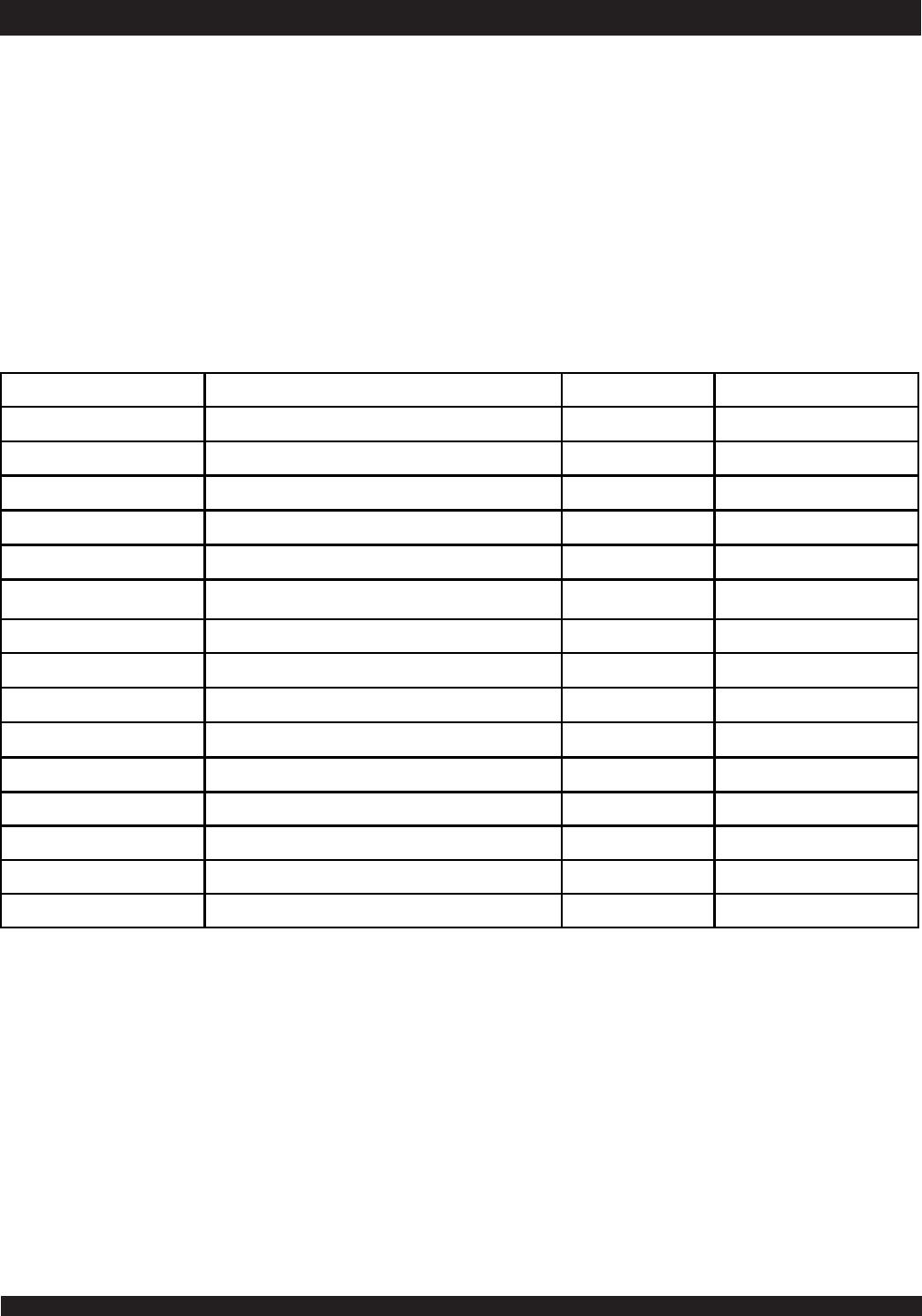
IDT71V67703, IDT71V67903, 256K x 36, 512K x 18, 3.3V Synchronous SRAMS with
3.3V I/O, Flow-Through Outputs, Single Cycle Deselect Commercial and Industrial Temperature Ranges
Symbol Pin Function I/O Active Description
A
0
-A
18
Address Inputs I N/A Synchronous Address inputs. The address register is triggered by a combi-nation of the
rising edge of CLK and ADSC Low or ADSP Low and CE Low.
ADSC
Address Status
(Cache Controller)
I LOW Synchronous Address Status from Cache Controller. ADSC is an active LOW input that is
used to load the address registers with new addresses.
ADSP
Address Status
(Processor)
I LOW Synchronous Address Status from Processor. ADSP is an active LOW input that is used to
load the address registers with new addresses. ADSP is gated by CE.
ADV
Burst Address
Advance
I LOW Synchronous Address Advance. ADV is an active LOW input that is used to advance the
internal burst counter, controlling burst access after the initial address is loaded. When the
input is HIGH the burst counter is not incremented; that is, there is no address advance.
BWE
Byte Write Enable I LOW Synchronous byte write enable gates the byte write inputs BW
1
-BW
4
. If BWE is LOW at the
rising edge of CLK then BWx inputs are passed to the next stage in the circuit. If BWE is
HIGH then the byte write inputs are blocked and only GW can initiate a write cycle.
BW
1
-BW
4
Individual Byte
Write Enables
I LOW Synchronous byte write enables. BW
1
controls I/O
0-7
, I/O
P1
, BW
2
controls I/O
8-15
, I/O
P2
, etc.
Any active byte write causes all outputs to be disabled.
CE
Chip Enable I LOW Synchronous chip enable. CE is used with CS
0
and CS
1
to enable the IDT71V67703/7903.
CE also gates ADSP.
CLK Clock I N/A This is the clock input. All timing references for the device are made with respect to this
input.
CS
0
Chip Select 0 I HIGH Synchronous active HIGH chip select. CS
0
is used with CE and CS
1
to enable the chip.
CS
1
Chip Select 1 I LOW Synchronous active LOW chip select. CS
1
is used with CE and CS
0
to enable the chip.
GW
Global Write
Enable
I LOW Synchronous global write enable. This input will write all four 9-bit data bytes when LOW
on the rising edge of CLK. GW supersedes individual byte write enables.
I/O
0
-I/O
31
I/O
P1
-I/O
P4
Data Input/Output I/O N/A Synchronous data input/output (I/O) pins. The data input path is registered, triggered by
the rising edge of CLK. The data output path is flow-through (no output register).
LBO
Linear Burst Order I LOW Asynchronous burst order selection input. When LBO is HIGH, the inter-leaved burst
sequence is selected. When LBO is LOW the Linear burst sequence is selected. LBO is a
static input and must not change state while the device is operating.
OE
Output Enable I LOW Asynchronous output enable. When OE is LOW the data output drivers are enabled on the
I/O pins if the chip is also selected. When OE is HIGH the I/O pins are in a high-
impedance state.
V
DD
Power Supply N/A N/A 3.3V core power supply.
V
DDQ
Power Supply N/A N/A 3.3V I/O Supply.
V
SS
Ground N/A N/A Ground.
NC No Connect N/A N/A NC pins are not electrically connected to the device.
ZZ Sleep Mode 1 HIGH Asynchronous sleep mode input. ZZ HIGH will gate the CLK internally and power down
the IDT71V67703/7903 to its lowest power consumption level. Data retention is guaranteed
in Sleep Mode.
5309 tbl 02
Pin Definitions
(1)
NOTE:
1. All synchronous inputs must meet specified setup and hold times with respect to CLK.