6.424
IDT71V67703, IDT71V67903, 256K x 36, 512K x 18, 3.3V Synchronous SRAMS with
3.3V I/O, Flow-Through Outputs, Single Cycle Deselect Commercial and Industrial Temperature Ranges
100-Pin TQFP Capacitance
(TA = +25° C, f = 1.0MHz)
Recommended Operating
Temperature Supply Voltage
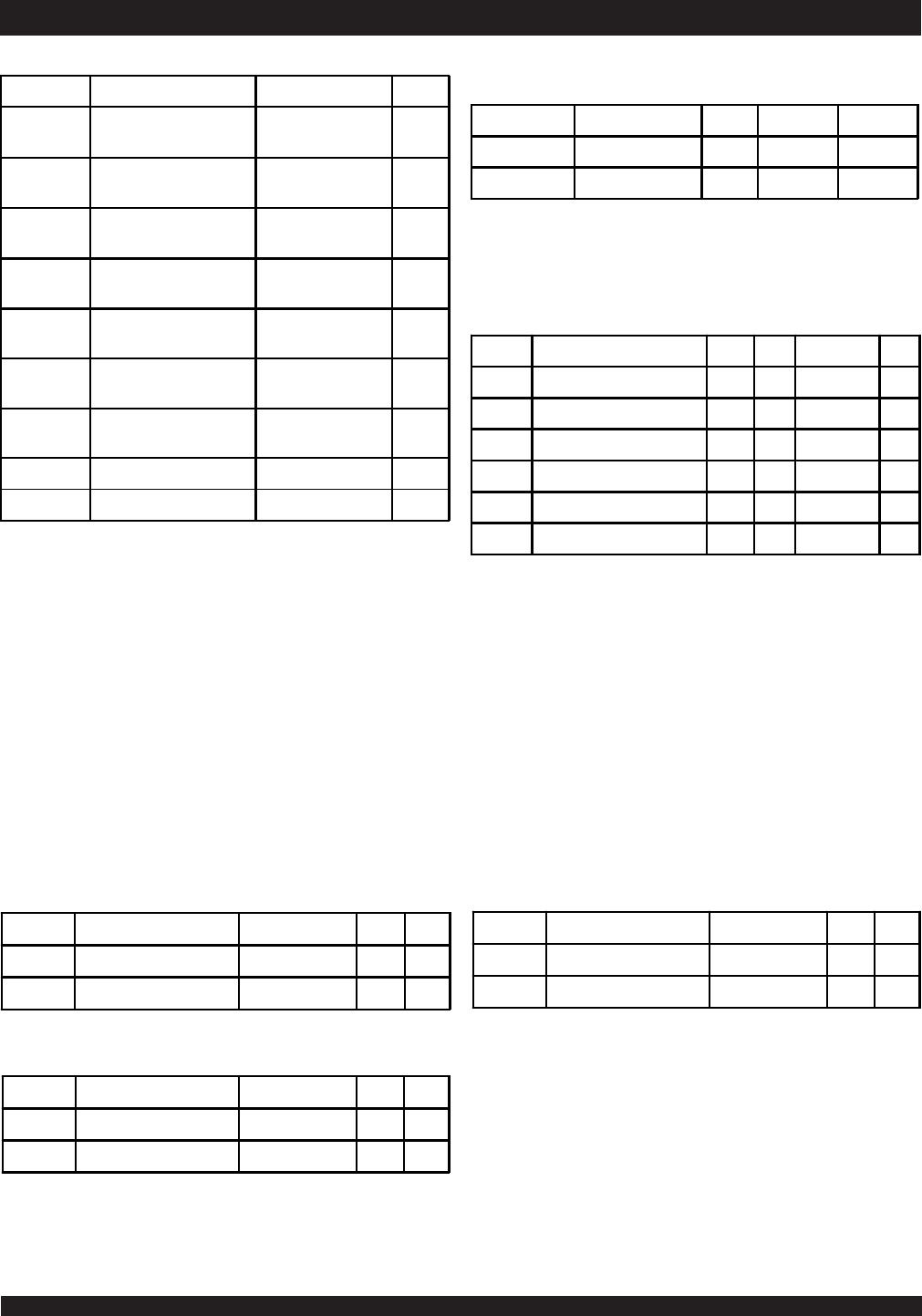
Absolute Maximum Ratings
(1)
NOTES:
1. Stresses greater than those listed under ABSOLUTE MAXIMUM RATINGS may
cause permanent damage to the device. This is a stress rating only and functional
operation of the device at these or any other conditions above those indicated
in the operational sections of this specification is not implied. Exposure to absolute
maximum rating conditions for extended periods may affect reliability.
2. VDD terminals only.
3. VDDQ terminals only.
4. Input terminals only.
5. I/O terminals only.
6. This is a steady-state DC parameter that applies after the power supplies have
ramped up. Power supply sequencing is not necessary; however, the voltage
on any input or I/O pin cannot exceed VDDQ during power supply ramp up.
7. TA is the "instant on" case temperature.
Recommended DC Operating
Conditions
NOTE:
1. VIL (min) = -1.0V for pulse width less than tCYC/2, once per cycle.
NOTE:
1. This parameter is guaranteed by device characterization, but not production tested.
Symbol Rating Commercial Unit
V
TE R M
(2 )
Terminal Voltage with
Respect to GND
-0.5 to +4.6 V
V
TE R M
(3,6)
Terminal Voltage with
Respect to GND
-0.5 to V
DD
V
V
TE R M
(4,6)
Terminal Voltage with
Respect to GND
-0.5 to V
DD
+0.5 V
V
TE R M
(5,6)
Terminal Voltage with
Respect to GND
-0.5 to V
DDQ
+0.5 V
T
A
(7)
Operating Temperature
-0 to +70
o
C
T
BIAS
Temperature
Under Bias
-55 to +125
o
C
T
STG
Storage
Temperature
-55 to +125
o
C
P
T
Power Dissipation 2.0 W
I
OUT
DC Output Current 50 mA
5309 tbl 03
Grade Temperature
(1)
V
SS
V
DD
V
DDQ
Commercial 0°C to +70°C 0V 3.3V±5% 3.3V±5%
Industrial -40°C to +85°C 0V 3.3V±5% 3.3V±5%
5309 tbl 04
Symbol Parameter Min. Typ. Max. Unit
V
DD
Core Supply Voltage 3.135 3.3 3.465 V
V
DDQ
I/O Supply Voltage 3.135 3.3 3.465 V
V
SS
Supply Voltage 0 0 0 V
V
IH
Input High Voltage - Inputs 2.0
____
V
DD
+0.3 V
V
IH
Input High Voltage - I/O 2.0
____
V
DDQ
+0.3 V
V
IL
Input Low Voltage -0.3
(1)
____
0.8 V
5309 tbl 05
Symbol Parameter
(1 )
Conditions Max. Unit
C
IN
Input Capacitance V
IN
= 3dV 5 pF
C
I/O
I/O Capacitance V
OUT
= 3dV 7 pF
5309 tbl 07
Symbol Parameter
(1)
Conditions Max. Unit
C
IN
Input Capacitance V
IN
= 3dV 7 pF
C
I/ O
I/O Capacitance V
OUT
= 3dV 7 pF
5309 tbl 07a
119 BGA Capacitance
(TA = +25° C, f = 1.0MHz)
NOTE:
1. T
A is the "instant on" case temperature.
165 fBGA Capacitance
(TA = +25° C, f = 1.0MHz)
Symbol Parameter
(1)
Conditions Max. Unit
C
IN
Input Capacitance V
IN
= 3dV 7 pF
C
I/ O
I/O Capacitance V
OUT
= 3dV 7 pF
5309 tbl 07b

