LT1116CS8#PBF

LT1116
1
1116fc
For more information www.linear.com/LT1116
Typical applicaTion
FeaTures DescripTion
12ns, Single Supply
Ground-Sensing Comparator
The LT
®
1116 is an ultra fast (12ns) comparator designed
for sensing signals near the negative supply. The input
common mode range extends from 2.5V below the
posi tive supply down to the negative supply rail. Like
the LT1016, this comparator is specifically designed to
inter face directly to TTL logic with complementary
outputs. The comparator may operate from either a single
5V supply or dual ±5V supplies. Tight offset voltage
specifi cations and high gain allow the LT1116 to be used
in precision applications.
The LT1116 is designed for improved speed and stability
for a wide range of operating conditions. The output stage
provides active drive in both directions for maximum speed
into TTL logic or passive loads, yet it has minimal cross-
conduction current. Unlike other fast comparators, the
LT1116 remains stable even for slow transitions through
the active region, which eliminates the need to specify a
minimum input slew rate.
The LT1116 has an internal, TTL compatible latch for
retaining data at the outputs. The latch holds data as
long as the latch pin is held high. Device parameters
such as gain, offset, and negative power supply current
are not significantly affected by variations in negative
supply voltage.
applicaTions
n
Ultra Fast (12ns Typ)
n
Operates off Single 5V Supply or ±5V
n
Input Common Mode Extends to Negative Supply
n
No Minimum Input Slew Rate Requirement
n
Complementary TTL Output
n
Inputs Can Exceed the Positive Supply Up to 15V
without Damaging the Comparator
n
Low Offset Voltage
n
Pin-Compatible with LT1016
n
Output Latch Capability
Available in 8-Lead PDIP and SO Packages
n
High Speed A/D Converters
n
Zero Crossing Detectors
n
Current Sense for Switching Regulators
n
Extended Range V to F Converters
n
Fast Pulse Height/Width Discriminators
n
High Speed Triggers
n
Line Receivers
n
High Speed Sampling Circuits
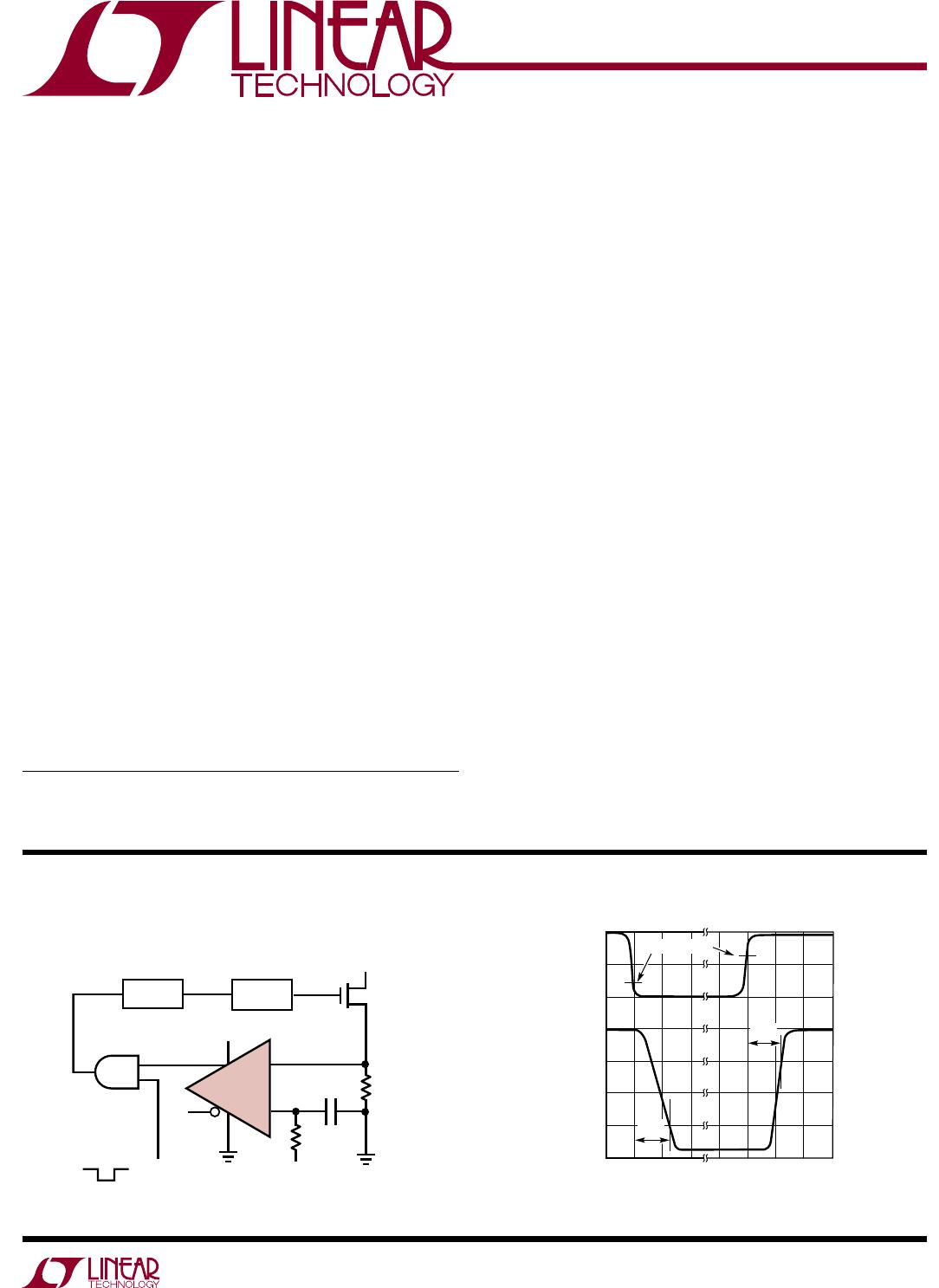
Fast Current Comparator for
Current Mode Switching Regulator
Comparator Response Time
LT1116 • TA01
LT1116
M1
C1
DRIVER
CONTROL INPUT
R
SENSE
BLANKING
LOGIC
Q
Q
R1
5V
+
TIME (ns)
OUTPUT
VOLTAGE V
OUT
1V/DIV
V
IN
100mV STEP
5mV OVERDRIVE
20 20
0 0
LT1116 • TA02
12ns
12ns
THRESHOLD
L, LTC, LT, and LTM are registered trademarks of Linear Technology Corporation.
All other trademarks are the property of their respective owners.
LT1116
2
1116fc
For more information www.linear.com/LT1116
absoluTe MaxiMuM raTings
Supply Voltage (V
+
) to GND ........................................7V
Negative Supply Voltage (V
) ....................... 7V to GND
Voltage
Differential Input Voltage .................................... ±15V
Inputs Voltage (Either Input) ...........(V
) –0.3V to 15V
(Note 1)
pin conFiguraTion
1
2
3
4
8
7
6
5
TOP VIEW
Q OUT
Q OUT
GND
V
+
+IN
IN
V
N8 PACKAGE
8-LEAD PDIP
T
JMAX
= 100°C, θ
JA
= 130°C/W
LATCH
ENABLE
+
1
2
3
4
8
7
6
5
TOP VIEW
Q OUT
Q OUT
GND
V
+
+IN
IN
V
S8 PACKAGE
8-LEAD PLASTIC SO
T
JMAX
= 100°C, θ
JA
= 160°C/W
LATCH
ENABLE
+
orDer inForMaTion
TUBE TAPE AND REEL PART MARKING* PACKAGE DESCRIPTION SPECIFIED TEMPERATURE RANGE
LT1116CN8#PBF NA 1116 8-Lead PDIP 0°C to 70°C
LT1116CS8#PBF LT1116CS8#TRPBF 1116 8-Lead Plastic SO 0°C to 70°C
Consult LTC Marketing for parts specified with wider operating temperature ranges.*The temperature grade is identified by a label on the shipping container.
Parts ending with PBF are RoHS and WEEE compliant.
For more information on tape and reel specifications, go to: http://www.linear.com/tapeandreel/. Some packages are available in 500 unit reels through
designated sales channels with #TRMPBF suffix.
Latch Pin Voltage .............................Equal to Supplies
Output Current (Continuous)
............................... ± 20mA
Operating Temperature Range
..................... 0°C to 70°C
Storage Temperature Range
..................65°C to 150°C
Lead Temperature (Soldering, 10 sec) ...................300°C
LT1116
3
1116fc
For more information www.linear.com/LT1116
SYMBOL PARAMETER CONDITIONS MIN TYP MAX UNITS
V
OS
Input Offset Voltage R
S
100Ω (Note 2)
l
1.0 ±3.0
3.5
mV
mV
ΔV
OS
ΔT
Input Offset Voltage Drift
l
5 µV/°C
I
OS
Input Offset Current (Note 2)
l
0.5 2 µA
l
B
Input Bias Current, Sourcing (Note 3)
l
10 20 µA
Input Voltage Range Arbitrary Supply Range
Single 5V Supply
l
l
V
0
(V
+
) –2.5
2.5
V
V
CMRR Common Mode Rejection Ratio 5V ≤ V
CM
≤ 2.5V, V
S
= ±5V
0V ≤ V
CM
≤ 2.5V
l
l
75
65
90
90
dB
dB
PSRR Power Supply Rejection Ratio Positive Supply, 4.6V ≤ V
+
≤ 5.4V
Negative Supply, –7 ≤ V
≤ –2V
l
l
60
80
75
100
dB
dB
A
V
Small Signal Voltage Gain 1V ≤ V
OUT
≤ 2V 1400 3000 V/V
I
+
Positive Supply Current
l
27 38 mA
I
Negative Supply Current
l
5 7 mA
V
OH
Output High Voltage I
SOURCE
= 1mA
I
SOURCE
= 10mA
l
l
2.7
2.4
3.4
3.0
V
V
V
OL
Output Low Voltage l
SINK
= 4mA
l
SINK
= 10mA
l
0.3
0.4
0.5 V
V
V
IH
+ Positive Latch Threshold
l
2.0 V
V
IL
Latch Threshold
l
0.8 V
I
IL
Latch Input Current V
LATCH
= 0V
l
–20 –500 µA
t
PD
Propagation Delay ∆V
IN
= 100mV, OD = 5mV (Note 4)
l
12 16
18
ns
ns
t
PD
Propagation Delay ∆V
IN
= 100mV, OD = 20mV (Note 4)
l
10 14
16
ns
ns
∆t
PD
Differential Propagation Delay ∆V
IN
= 100mV, OD = 5mV (Note 4) 3 ns
t
SU
Latch Set-Up Time (Note 5) 2 ns
t
H
Latch Hold Time (Note 5) 2 ns
elecTrical characTerisTics
The l denotes the specifications which apply over full operating temperature
range, otherwise specifications are at T
A
= 25°C. V
+
= 5V, V
= –5V, V
OUT
(Q) = 1.4V, LATCH = 0V. Specifications for V
OS
, I
B
, CMRR,
and Voltage Gain are valid for single supply operation, V
+
= 5V, V
= 0V, unless noted.
Note 1: Stresses beyond those listed under Absolute Maximum Ratings
may cause permanent damage to the device. Exposure to any Absolute
Maximum Rating condition for extended periods may affect device
reliability and lifetime.
Note 2: Input offset voltage is defined as the average of two offset
voltages measured by forcing first the Q output to 1.4V then forcing
the Q output to 1.4V.
Note 3
:
Input bias current is defined as the average of the two input
currents.
Note 4: t
PD
and ∆t
PD
cannot be measured in automatic handling equipment
with low values of overdrive. The LT1116 is sample tested with a 1V step
and 500mV overdrive. Correlation tests have shown that t
PD
and ∆t
PD
can
be guaranteed with this test if additional DC tests are performed to verify
internal bias conditions are correct. For low overdrive conditions V
OS
is
added to the measured overdrive.
Note 5: Input latch set-up time, t
SU
, is the interval in which the input signal
must be stable prior to asserting the latch signal. The hold time,
t
H
, is the interval after the latch is asserted in which the input signal must
be stable.

LT1116CS8#PBF

Mfr. #:
Manufacturer:
Analog Devices Inc.
Description:
Analog Comparators 12ns Ground Sensing Comparator
Lifecycle:
New from this manufacturer.
Delivery:
DHL FedEx Ups TNT EMS
Payment:
T/T Paypal Visa MoneyGram Western Union

Products related to this Datasheet