LT1116CS8#PBF

LT1116
7
1116fc
For more information www.linear.com/LT1116
Input Characteristics
Each input to the LT1116 is buffered with a fast PNP
followerinput bias current therefore does not vary
significantly throughout the common mode range. When
either input exceeds the positive common mode limit, the
bias current drops to zero. Inputs that fall more than one
diode and drop below V
will forward bias the substrate
or clamp diode, causing large input current to flow.
Single ended input resistance is about 5MΩ, and re
-
mains roughly constant over the input common mode
range. The common mode resistance is about 2.5MΩ
with zero differential input voltage, and does not change
signifi cantly with the absolute value of differential input.
Effective input capacitance, typically 5pF, is determined
by measuring the resulting change in propagation delay
for a 1kΩ change in source resistance.
applicaTions inForMaTion
Latch Pin Dynamics
The internal latch uses local regenerative feedback to
shorten set-up and hold times. Driving the latch pin high
retains the output state. The latch pin floats to a high
state when disconnected, so it must be driven low for
flow-through operation. The set-up time required to
guarantee detecting a given transition of the inputs is 2ns.
The inputs must also remain stable for a
2ns hold time
after latch is asserted. New data will appear at the output
approximately 10ns to 12ns after the latch goes low. The
latch pin has no built-in hysteresis, and is designed to be
driven from TTL or CMOS logic gates.
Additional Information
Linear Technologys Application Note 13 provides an
extensive discussion of design techniques for high speed
comparators.
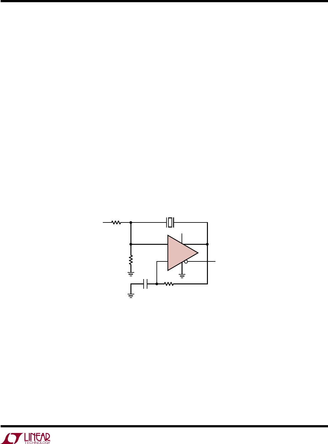
Figure 2. This Single Supply Crystal Oscillator Utilizes Crystals
From 10MHz To 15MHz Without Component Changes
Single Supply Crystal Oscillator 10MHz to 15MHz
LT1116 • AI02
Q
OUTPUT
2kΩ
1kΩ
1kΩ
24pF
5V
10 TO 15MHz
AT CUT
5V
Q
LT1116
+
LT1116
8
1116fc
For more information www.linear.com/LT1116
applicaTions inForMaTion
High Speed Adaptive Trigger Circuit
Line receivers often require an adaptive trigger to
compen
sate for variations in signal amplitude and DC
offsets. The circuit in Figure 3 triggers on 2mV to 200mV
signals from 100Hz to 10MHz from a single 5V rail. The
trigger level is the average of the input signals positive
and negative peaks stored on 0.005µF capacitors. Pairs of
NPN and PNP transistors are used instead of diodes to
temperature compensate the peak detector
.
T
o achieve single supply operation, the input signal
must be shifted into the pre-amplifiers common mode
range. The input amplifier A1 adds a 1V level shift, while
A2 provides a gain of 20 for high frequency signals.
Capaci tors C1 and C2 insure that low frequency signals
see unity gain. Bandwidth limiting in A1 and A2 does not
affect triggering because the adaptive trigger threshold
varies ratiometrically to maintain circuit output.
+
+
+
LT1116 • AI03
Q
500Ω
200Ω
4R
200Ω
R
100Ω
50Ω
1kΩ
1kΩ
1kΩ
3kΩ
1%
3kΩ
1%
500pF
5pF
1000pF
3MΩ
3MΩ
0.1µF
47µF
C1
100µF
C2
0.1µF
0.005µF
0.005µF
5V
5V
5V
5V
5V
5V
LT1116
A2
LT1192
A1
LT1191
A3
LT1006
+
Q
CABLE
V
IN
NPN = 2N3904
PNP = 2N3906
TRIGGER
OUT
Figure 3. Fast Single Supply Adaptive Trigger
LT1116
9
1116fc
For more information www.linear.com/LT1116
revision hisTory
REV DATE DESCRIPTION PAGE NUMBER
C 02/16 Addition of Web Links
Reformat of Order Information
Correction to Electrical Characteristics Conditions, V
= –5V
2
All
3
(Revision history begins at Rev C)
Information furnished by Linear Technology Corporation is believed to be accurate and reliable.
However, no responsibility is assumed for its use. Linear Technology Corporation makes no representa-
tion that the interconnection of its circuits as described herein will not infringe on existing patent rights.

LT1116CS8#PBF

Mfr. #:
Manufacturer:
Analog Devices Inc.
Description:
Analog Comparators 12ns Ground Sensing Comparator
Lifecycle:
New from this manufacturer.
Delivery:
DHL FedEx Ups TNT EMS
Payment:
T/T Paypal Visa MoneyGram Western Union

Products related to this Datasheet