LT1116
6
1116fc
For more information www.linear.com/LT1116
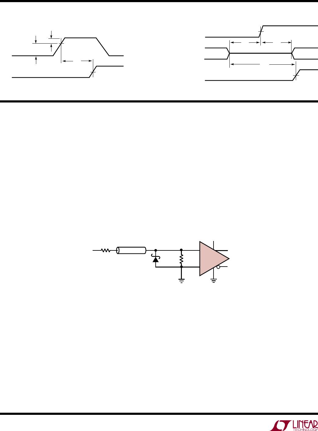
Figure 1.
The Zero Crossing Detector Terminates the Transmission Line at Its 50Ω Characteristic
Impedance. Negative Inputs Should Not Fall Below –2V to Keep the Signal Current Within the
Clamp Diode’s Maximum Forward Rating. Positive Inputs Should not Exceed the Device’s Absolute
Maximum Ratings nor the Power Rating on the Terminating Resistor
CABLE
1N5712
IN
R
S
50
R
T
50Ω
LT1116
+
–
Fast Zero Crossing Detector
TiMing DiagraM
applicaTions inForMaTion
OD
∆V
INV
IN
OUT
t
PD
V
IN
LATCH
t
SU
t
PD
t
H
V
OUT
Common Mode Considerations
The LT1116 is specified for a common mode range of
0V to 2.5V with a single 5V supply, and –5V to 2.5V with
±5V supplies. The common mode range is defined as the
DC input for which the output responds correctly to small
changes in the input differential. Input signals can exceed
the positive common mode limit up to the 15V absolute
maximum rating without damaging the comparator. There
will, however, be an increase in propagation delay of up
to 10ns when the input signal switches back into the
com mon mode range. When input signals fall below the
negative common mode limit, the internal PN diode formed
with the substrate can turn on (resulting in significant
charge flow throughout the die). A Schottky clamp diode,
between the input and the negative rail, speeds up recovery
from negative overdrive by preventing the substrate diode
from turning on. The zero crossing detector in Figure 1
demonstrates the use of a fast clamp diode. Recovery,
from 500mV overdrive below V
–
, for this circuit is ap-
proximately 18ns.