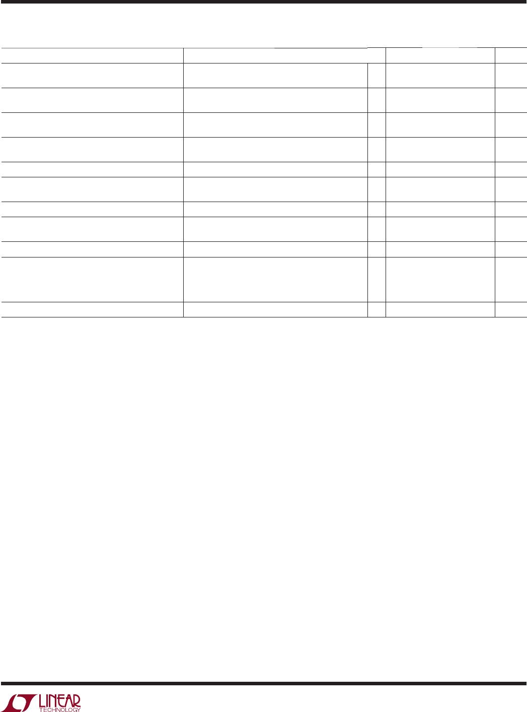
LT3082
1
3082f
TYPICAL APPLICATION
DESCRIPTION
200mA Single Resistor Low
Dropout Linear Regulator
The LT
®
3082 is a 200mA low dropout linear regulator that
can be paralleled to increase output current or spread heat
in surface mounted boards. Architected as a precision
current source and voltage follower, this regulator benefi ts
many applications requiring high current, adjustability to
zero and no heat sink. The LT3082 withstands reverse
input voltages and reverse output-to-input voltages without
reverse-current fl ow.
A key feature of the LT3082 is the capability to supply a
wide output voltage range. A precision “0” TC 10µA ref-
erence current source drives a single resistor to program
the output voltage to any level between zero and 38.5V.
The LT3082 is stable with only 2.2µF of capacitance on
the output; the IC uses small ceramic capacitors that
do not require additional ESR as is common with other
regulators.
Internal protection circuitry includes reverse-battery and
reverse-current protection, current limiting and ther-
mal limiting. The LT3082 is offered in the thermally en-
hanced 8-lead TSOT-23, 3-lead SOT-223 and 8-lead 3mm
× 3mm DFN packages.
Variable Output Voltage Battery Powered Supply
FEATURES
APPLICATIONS
n
Outputs May Be Paralleled for Higher Output
Current or Heat Spreading
n
Maximum Output Current: 200mA
n
Wide Input Voltage Range: 1.2V to 40V
n
Output Adjustable to 0V
n
Stable with Minimum 2.2μF Ceramic Capacitors
n
Single Resistor Sets Output Voltage
n
Initial Set Pin Current Accuracy: 1%
n
Low Output Noise: 33μV
RMS
(10Hz to 100kHz)
n
Reverse-Battery Protection
n
Reverse-Current Protection
n
<1mV Load Regulation Typical
n
<0.001%/V Line Regulation Typical
n
Current Limit and Thermal Shutdown Protection
n
Available in 8-Lead SOT-23, 3-Lead SOT-223 and
8-Lead 3mm × 3mm DFN Packages
n
All-Surface Mount Power Supply
n
Post Regulator for Switching Supplies
n
Low Parts Count Variable Voltage Supply
n
Low Output Voltage Supply
n
Battery Powered Regulator
SET Pin Current vs Temperature
L, LT, LTC, LTM, Linear Technology and the Linear logo are registered trademarks of Linear
Technology Corporation. All other trademarks are the property of their respective owners.
TEMPERATURE (°C)
–50
9.900
SET PIN CURRENT (µA)
9.950
10.000
10.050
–25
0
25 50 10075 125
10.100
9.925
9.975
10.025
10.075
150
3082 TA01b
3082 TA01a
IN
SET OUT
+
LT3082
V
OUT
= 10µA • R
SET
C
SET
0.1µF
R
SET
500k
F
10µA
9V
C
OUT
2.2µF
LT3082
2
3082f
PIN CONFIGURATION
ABSOLUTE MAXIMUM RATINGS
IN Pin Voltage Relative to SET, OUT ........................±40V
SET Pin Current (Note 6) .....................................±15mA
SET Pin Voltage (Relative to OUT, Note 6) ...............±10V
Output Short-Circuit Duration .......................... Indefi nite
(Note 1) All Voltages Relative to V
OUT
TOP VIEW
DD PACKAGE
8-LEAD (3mm s 3mm) PLASTIC DFN
5
6
7
8
9
4
3
2
1OUT
OUT
NC
SET
IN
IN
NC
NC
T
JMAX
= 125°C, θ
JA
= 28°C/W, θ
JC
= 3°C/W
EXPOSED PAD (PIN 9) IS OUT, MUST BE SOLDERED TO OUT ON
THE PCB; SEE THE APPLICATIONS INFORMATION SECTION
3
2
1
TOP VIEW
TAB IS OUT
IN
OUT
SET
ST PACKAGE
3-LEAD PLASTIC SOT-223
T
JMAX
= 125°C, θ
JA
= 24°C/W, θ
JC
= 15°C/W
TAB IS OUT, MUST BE SOLDERED TO OUT ON THE PCB;
SEE THE APPLICATIONS INFORMATION SECTION
NC 1
OUT 2
OUT 3
OUT 4
8 IN
7 IN
6 NC
5 SET
TOP VIEW
TS8 PACKAGE
8-LEAD PLASTIC TSOT-23
T
JMAX
= 125°C, θ
JA
= 57°C/W, θ
JC
= 15°C/W
ORDER INFORMATION
LEAD FREE FINISH TAPE AND REEL PART MARKING* PACKAGE DESCRIPTION TEMPERATURE RANGE
LT3082EDD#PBF LT3082EDD#TRPBF LDYT
8-Lead (3mm × 3mm) Plastic DFN
–40°C to 125°C
LT3082IDD#PBF LT3082IDD#TRPBF LDYT
8-Lead (3mm × 3mm) Plastic DFN
–40°C to 125°C
LT3082EST#PBF LT3082EST#TRPBF 3082 3-Lead Plastic SOT-223 –40°C to 125°C
LT3082IST#PBF LT3082IST#TRPBF 3082 3-Lead Plastic SOT-223 –40°C to 125°C
LT3082MPST#PBF LT3082MPST#TRPBF 3082MP 3-Lead Plastic SOT-223 –55°C to 125°C
LT3082ETS8#PBF LT3082ETS8#TRPBF LTDYV 8-Lead Plastic SOT-23 –40°C to 125°C
LT3082ITS8#PBF LT3082ITS8#TRPBF LTDYV 8-Lead Plastic SOT-23 –40°C to 125°C
LEAD BASED FINISH TAPE AND REEL PART MARKING* PACKAGE DESCRIPTION TEMPERATURE RANGE
LT3082EDD LT3082EDD#TR LDYT
8-Lead (3mm × 3mm) Plastic DFN
–40°C to 125°C
LT3082IDD LT3082IDD#TR LDYT
8-Lead (3mm × 3mm) Plastic DFN
–40°C to 125°C
LT3082EST LT3082EST#TR 3082 3-Lead Plastic SOT-223 –40°C to 125°C
LT3082IST LT3082IST#TR 3082 3-Lead Plastic SOT-223 –40°C to 125°C
LT3082MPST LT3082MPST#TR 3082MP 3-Lead Plastic SOT-223 –55°C to 125°C
LT3082ETS8 LT3082ETS8#TR LTDYV 8-Lead Plastic SOT-23 –40°C to 125°C
LT3082ITS8 LT3082ITS8#TR LTDYV 8-Lead Plastic SOT-23 –40°C to 125°C
Consult LTC Marketing for parts specifi ed with wider operating temperature ranges. *The temperature grade is identifi ed by a label on the shipping container.
For more information on lead free part marking, go to:
http://www.linear.com/leadfree/
For more information on tape and reel specifi cations, go to: http://www.linear.com/tapeandreel/
Operating Junction Temperature Range (Notes 2, 8)
E, I Grades ......................................... –40°C to 125°C
MP Grade ........................................... –55°C to 125°C
Storage Temperature Range ................... –65°C to 150°C
Lead Temperature (ST, TS8 Packages Only)
Soldering, 10 sec .............................................. 300°C
LT3082
3
3082f
ELECTRICAL CHARACTERISTICS
The l denotes the specifi cations which apply over the full operating
temperature range, otherwise specifi cations are at T
J
= 25°C. (Note 2)
Note 1: Stresses beyond those listed under Absolute Maximum Ratings
may cause permanent damage to the device. Exposure to any Absolute
Maximum Rating condition for extended periods may affect device
reliability and lifetime.
Note 2: Unless otherwise specifi ed, all voltages are with respect to V
OUT
.
The LT3082E is tested and specifi ed under pulse load conditions such
that T
J
T
A
. The LT3082E is 100% tested at T
A
= 25°C. Performance at
–40°C and 125°C is assured by design, characterization, and correlation
with statistical process controls. The LT3082I is guaranteed to meet all
data sheet specifi cations over the full –40°C to 125°C operating junction
temperature range. The LT3082MP is 100% tested and guaranteed over
the –55°C to 125°C operating junction temperature range.
Note 3: Minimum load current is equivalent to the quiescent current of
the part. Since all quiescent and drive current is delivered to the output
of the part, the minimum load current is the minimum current required to
maintain regulation.
Note 4: For the LT3082, dropout is specifi ed as the minimum input-to-
output voltage differential required supplying a given output current.
Note 5: Adding a small capacitor across the reference current resistor
lowers output noise. Adding this capacitor bypasses the resistor shot
noise and reference current noise; output noise is then equal to error
amplifi er noise (see the Applications Information section).
Note 6: Diodes with series 1k resistors clamp the SET pin to the OUT pin.
These diodes and resistors only carry current under transient overloads.
Note 7: Load regulation is Kelvin-sensed at the package.
Note 8: This IC includes overtemperature protection that protects the
device during momentary overload conditions. Junction temperature
exceeds the maximum operating junction temperature when
overtemperature protection is active. Continuous operation above the
specifi ed maximum operating junction temperature may impair device
reliability.
PARAMETER CONDITIONS MIN TYP MAX UNITS
SET Pin Current I
SET
V
IN
= 2V, I
LOAD
= 1mA
2V ≤ V
IN
≤ 40V, 1mA ≤ I
LOAD
≤ 200mA
l
9.90
9.80
10
10
10.10
10.20
µA
µA
Offset Voltage (V
OUT
– V
SET
) V
OS
V
IN
= 2V, I
LOAD
= 1mA
V
IN
= 2V, I
LOAD
= 1mA
l
–2
–4
2
4
mV
mV
Load Regulation (Note 7) ∆I
SET
∆V
OS
∆I
LOAD
= 1mA to 200mA
∆I
LOAD
= 1mA to 200mA
l
–0.1
–0.5 –2
nA
mV
Line Regulation ∆I
SET
∆V
OS
∆V
IN
= 2V to 40V, I
LOAD
= 1mA
∆V
IN
= 2V to 40V, I
LOAD
= 1mA
0.03
0.003
0.2
0.010
nA/V
mV/V
Minimum Load Current (Note 3) 2V ≤ V
IN
≤ 40V
l
300 500 µA
Dropout Voltage (Note 4) I
LOAD
= 10mA
I
LOAD
= 200mA
l
l
1.22
1.3
1.45
1.65
V
V
Current Limit V
IN
= 5V, V
SET
= 0V, V
OUT
= –0.1V
l
200 300 mA
Error Amplifi er RMS Output Noise (Note 5) I
LOAD
= 200mA, 10Hz ≤ f ≤ 100kHz, C
OUT
= 10µF,
C
SET
= 0.1µF
33 µV
RMS
Reference Current RMS Output Noise (Note 5) 10Hz ≤ f ≤ 100kHz 0.7 nA
RMS
Ripple Rejection f = 120Hz, V
RIPPLE
= 0.5V
P-P
, I
LOAD
= 0.1A,
C
OUT
= 2.2µF, C
SET
= 0.1µF
f = 10kHz
f = 1MHz
90
75
20
dB
dB
dB
Thermal Regulation I
SET
10ms Pulse 0.003 %/W

LT3082EST#PBF

Mfr. #:
Manufacturer:
Analog Devices / Linear Technology
Description:
LDO Voltage Regulators 200mA Programmable 2-Terminal Current Source or Linear Regulator
Lifecycle:
New from this manufacturer.
Delivery:
DHL FedEx Ups TNT EMS
Payment:
T/T Paypal Visa MoneyGram Western Union