LT3082
7
3082f
PIN FUNCTIONS
(DD/ST/TS8)
BLOCK DIAGRAM
IN
SET
10µA
3082 BD
OUT
+
IN (Pins 7, 8/Pin 3/Pins 7, 8): Input. This pin supplies
power to regulate internal circuitry and supply output load
current. For the device to operate properly and regulate,
the voltage on this pin must be 1.2V to 1.4V above the
OUT pin (depending on output load current—see the
dropout voltage specifi cations in the Electrical Charac-
teristics table).
NC (Pins 3, 5, 6/NA/Pins 1, 6): No Connection. These
pins have no connection to internal circuitry and may be
tied to IN, OUT, GND or fl oated.
OUT (Pins 1, 2/Pin 2/Pins 2, 3, 4): Output. This is the
power output of the device. The LT3082 requires a 0.5mA
minimum load current or the output will not regulate.
SET (Pin 4/Pin 1/Pin 5): Set. This pin is the error ampli-
ers noninverting input and also sets the operating bias
point of the circuit. A fi xed 10A current source fl ows
out of this pin. A single external resistor programs V
OUT
.
Output voltage range is 0V to 38.5V.
Exposed Pad/Tab (Pin 9/Tab/NA): Output. The Exposed
Pad of the DFN package and the Tab of the SOT-223
package are tied internally to OUT. Tie them directly to OUT
pins (Pins 1, 2/Pin 2) at the PCB. The amount of copper area
and planes connected to the Exposed Pad/Tab determine
the effective thermal resistance of the packages (see the
Applications Information section).
LT3082
8
3082f
Introduction
The LT3082 regulator is easy to use and has all the pro-
tection features expected in high performance regulators.
Included are reverse-input, reverse-output and reverse
input-to-output protection for sensitive circuitry and loads.
Additional protection includes short-circuit protection and
thermal shutdown with hysteresis.
The LT3082 fi ts well in applications needing multiple rails.
This new architecture adjusts down to zero with a single
resistor, handling modern low voltage digital IC’s as well
as allowing easy parallel operation and thermal manage-
ment without heat sinks. Adjusting to zero output allows
shutting off the powered circuitry. When the input is pre-
regulated—such as a 5V or 3.3V input supply—external
resistors can help spread the heat.
A precision “0” TC 10A reference current source connects
to the noninverting input of a power operational amplifi er.
The power operational amplifi er provides a low impedance
buffered output to the voltage on the noninverting input.
A single resistor from the noninverting input to ground
sets the output voltage. If this resistor is set to 0, zero
output voltage results. Therefore, any output voltage be-
tween zero and the maximum defi ned by the input power
supply voltage is obtainable.
The benefi t of using a true internal current source as the
reference, as opposed to a bootstrapped reference in older
regulators, is not so obvious in this architecture. A true
APPLICATIONS INFORMATION
reference current source allows the regulator to have gain
and frequency response independent of the impedance on
the positive input. On older adjustable regulators, such as
the LT1086, loop gain changes with output voltage and
bandwidth changes if the adjustment pin is bypassed
to ground. For the LT3082, loop gain is unchanged with
output voltage changes or bypassing. Output regulation
is not a fi xed percentage of output voltage, but is a fi xed
fraction of millivolts. Use of a true current source allows
all of the gain in the buffer amplifi er to provide regulation,
and none of that gain is needed to amplify up the reference
to a higher output voltage.
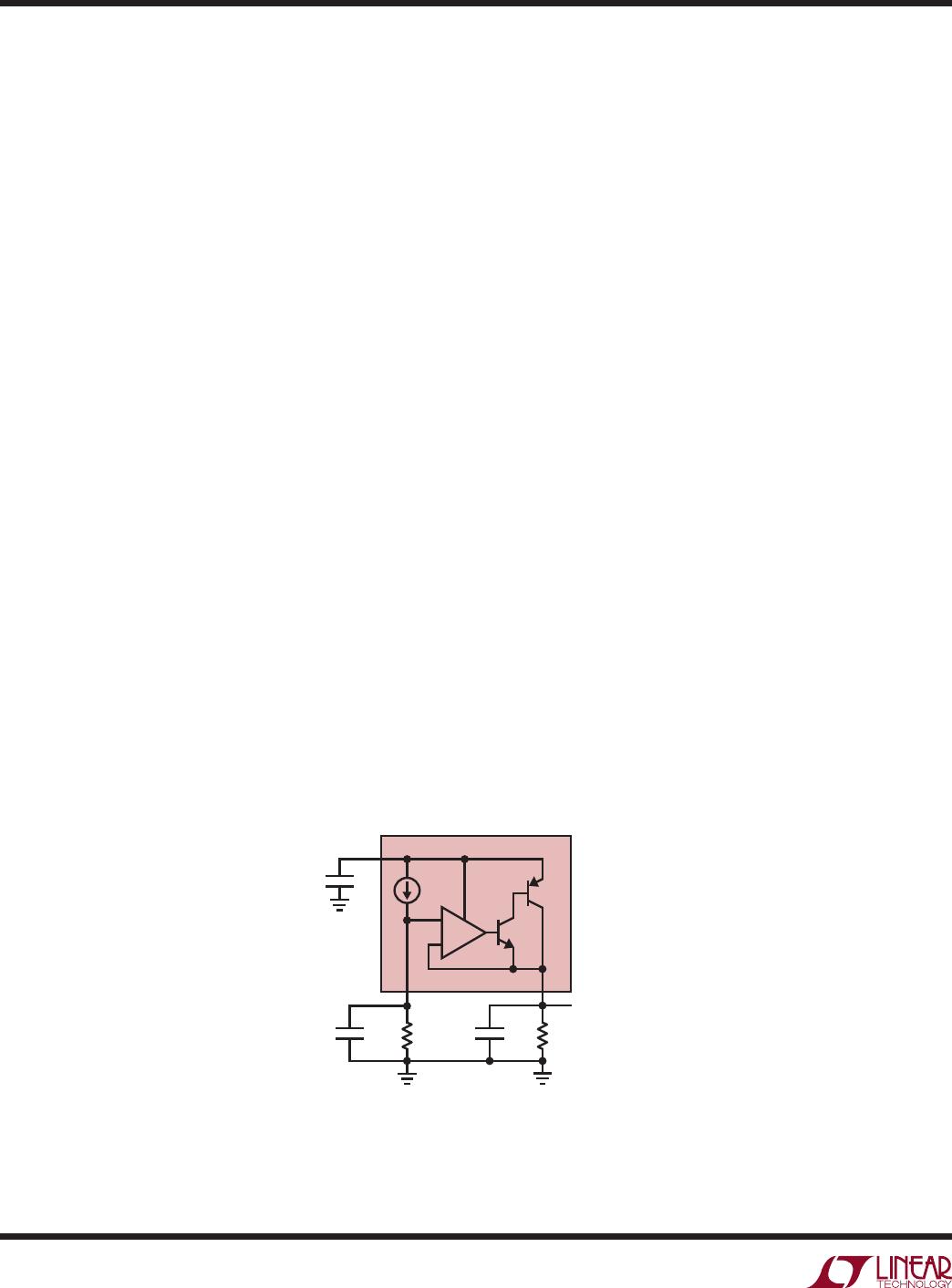
Programming Output Voltage
The LT3082 generates a 10A reference current that
ows out of the SET pin. Connecting a resistor from SET
to GND generates a voltage that becomes the reference
point for the error amplifi er (see Figure 1). The reference
voltage equals 10A multiplied by the value of the SET
pin resistor. Any voltage may be generated and there
is no minimum output voltage for the regulator. Table
1 lists many common output voltages and the closest
standard 1% resistor values used to generate that output
voltage.
Regulation of the output voltage requires a minimum load
current of 0.5mA. For a true 0V output operation, return
this minimum 0.5mA load current to a negative supply
voltage.
Figure 1. Basic Adjustable Regulator
3082 F01
IN
SET OUT
+
LT3082
10µA
R
LOAD
C
SET
R
SET
C
IN
V
OUT
= 10µA • R
SET
C
OUT
LT3082
9
3082f
APPLICATIONS INFORMATION
Table 1. 1% Resistors for Common Output Voltages
V
OUT
(V) R
SET
(k)
1 100
1.2 121
1.5 150
1.8 182
2.5 249
3.3 332
5 499
With a 10A current source generating the reference
voltage, leakage paths to or from the SET pin can create
errors in the reference and output voltages. High qual-
ity insulation should be used (e.g., Tefl on, Kel-F). The
cleaning of all insulating surfaces to remove fl uxes and
other residues may be required. Surface coating may be
necessary to provide a moisture barrier in high humidity
environments.
Minimize board leakage by encircling the SET pin and
circuitry with a guard ring that is operated at a potential
close to itself. Tie the guard ring to the OUT pin. Guarding
both sides of the circuit board is required. Bulk leakage
reduction depends on the guard ring width. 10nA of leak-
age into or out of the SET pin and its associated circuitry
creates a 0.1% reference voltage error. Leakages of this
magnitude, coupled with other sources of leakage, can
cause signifi cant offset voltage and reference drift, es-
pecially over the possible operating temperature range.
Figure 2 depicts an example guard ring layout.
If guard ring techniques are used, this bootstraps any
stray capacitance at the SET pin. Since the SET pin is
a high impedance node, unwanted signals may couple
into the SET pin and cause erratic behavior. This will
be most noticeable when operating with minimum
output capacitors at full load current. The easiest way
to remedy this is to bypass the SET pin with a small
amount of capacitance from SET to ground; 10pF to
20pF is suffi cient.
Stability and Output Capacitance
The LT3082 requires an output capacitor for stability. It
is designed to be stable with most low ESR capacitors
(typically ceramic, tantalum or low ESR electrolytic). A
minimum output capacitor of 2.2F with an ESR of 0.5
or less is recommended to prevent oscillations. Larger
values of output capacitance decrease peak deviations
and provide improved transient response for larger load
current changes. Bypass capacitors, used to decouple
individual components powered by the LT3082, increase
the effective output capacitor value. For improvement in
transient response performance, place a capacitor across
the voltage setting resistor. Capacitors up to 1F can be
used. This bypass capacitor reduces system noise as well,
but start-up time is proportional to the time constant of
the voltage setting resistor (R
SET
in Figure 1) and SET pin
bypass capacitor.
Give extra consideration to the use of ceramic capacitors.
Ceramic capacitors are manufactured with a variety of di-
Figure 2. Example Guard Ring Layout for DFN Package
3082 F02
OUT
GND
SET

LT3082EST#PBF

Mfr. #:
Manufacturer:
Analog Devices / Linear Technology
Description:
LDO Voltage Regulators 200mA Programmable 2-Terminal Current Source or Linear Regulator
Lifecycle:
New from this manufacturer.
Delivery:
DHL FedEx Ups TNT EMS
Payment:
T/T Paypal Visa MoneyGram Western Union