LT3082
10
3082f
APPLICATIONS INFORMATION
electrics, each with different behavior across temperature
and applied voltage. The most common dielectrics used
are specifi ed with EIA temperature characteristic codes of
Z5U, Y5V, X5R and X7R. The Z5U and Y5V dielectrics are
good for providing high capacitances in a small package,
but they tend to have strong voltage and temperature
coeffi cients, as shown in Figures 3 and 4. When used with
a 5V regulator, a 16V 10F Y5V capacitor can exhibit an
effective value as low as 1F to 2F for the DC bias voltage
applied and over the operating temperature range. The X5R
and X7R dielectrics result in more stable characteristics
and are more suitable for use as the output capacitor.
The X7R type has better stability across temperature,
while the X5R is less expensive and is available in higher
values. Care still must be exercised when using X5R and
X7R capacitors. The X5R and X7R codes only specify
operating temperature range and maximum capacitance
change over temperature. Capacitance change due to DC
bias with X5R and X7R capacitors is better than with Y5V
and Z5U capacitors, but can still be signifi cant enough to
drop capacitor values below appropriate levels. Capacitor
DC bias characteristics tend to improve as component
case size increases, but expected capacitance at operating
voltage should be verifi ed.
Voltage and temperature coeffi cients are not the only
sources of problems. Some ceramic capacitors have a
piezoelectric response. A piezoelectric device generates
voltage across its terminals due to mechanical stress. In a
ceramic capacitor, the stress can be induced by vibrations
in the system or thermal transients.
Stability and Input Capacitance
Low ESR, ceramic input bypass capacitors are acceptable
for applications without long input leads. However, applica-
tions connecting a power supply to an LT3082 circuit’s IN
and GND pins with long input wires combined with a low
ESR, ceramic input capacitors are prone to voltage spikes,
reliability concerns and application-specifi c board oscil-
lations. The input wire inductance found in many battery
powered applications, combined with the low ESR ceramic
input capacitor, forms a high-Q LC resonant tank circuit. In
some instances this resonant frequency beats against the
output current dependent LDO bandwidth and interferes
with proper operation. Simple circuit modifi cations/solu-
tions are then required. This behavior is not indicative of
LT3082 instability, but is a common ceramic input bypass
capacitor application issue.
The self-inductance, or isolated inductance, of a wire is
directly proportional to its length. Wire diameter is not a
major factor on its self-inductance. For example, the self-
inductance of a 2-AWG isolated wire (diameter = 0.26") is
about half the self-inductance of a 30-AWG wire (diameter
= 0.01"). One foot of 30-AWG wire has about 465nH of
self-inductance.
One of two ways reduces a wire’s self-inductance. One
method divides the current fl owing towards the LT3082
between two parallel conductors. In this case, the farther
apart the wires are from each other, the more the self-in-
ductance is reduced; up to a 50% reduction when placed
a few inches apart. Splitting the wires basically connects
DC BIAS VOLTAGE (V)
CHANGE IN VALUE (%)
3082 F03
20
0
–20
–40
–60
–80
–100
0
4
8
10
26
12
14
X5R
Y5V
16
BOTH CAPACITORS ARE 16V,
1210 CASE SIZE, 10µF
Figure 3. Ceramic Capacitor DC Bias Characteristics
TEMPERATURE (°C)
–50
40
20
0
–20
–40
–60
–80
–100
25 75
3082 F04
–25 0
50 100 125
Y5V
CHANGE IN VALUE (%)
X5R
BOTH CAPACITORS ARE 16V,
1210 CASE SIZE, 10µF
Figure 4. Ceramic Capacitor Temperature Characteristics
LT3082
11
3082f
APPLICATIONS INFORMATION
two equal inductors in parallel, but placing them in close
proximity gives the wires mutual inductance adding to
the self-inductance. The second and most effective way
to reduce overall inductance is to place both forward and
return current conductors (the input and GND wires) in
very close proximity. Two 30-AWG wires separated by
only 0.02", used as forward- and return-current conduc-
tors, reduce the overall self-inductance to approximately
one-fi fth that of a single isolated wire.
If wiring modifi cations are not permissible for the applica-
tions, including series resistance between the power supply
and the input of the LT3082 also stabilizes the application.
As little as 0.1 to 0.5, often less, is effective in damping
the LC resonance. If the added impedance between the
power supply and the input is unacceptable, adding ESR to
the input capacitor also provides the necessary damping of
the LC resonance. However, the required ESR is generally
higher than the series impedance required.
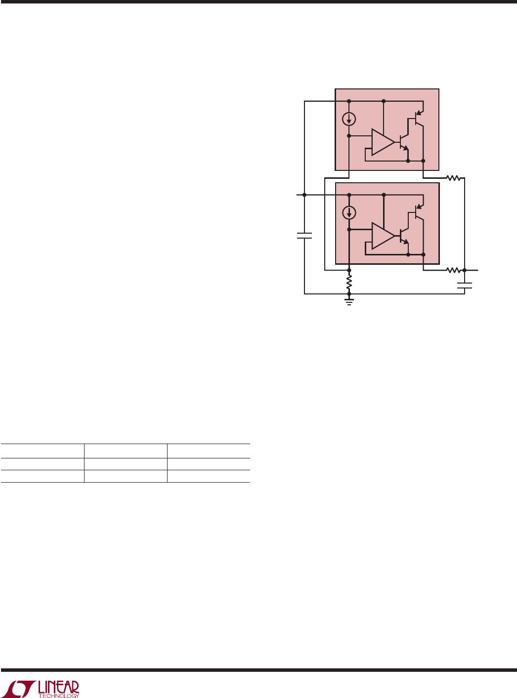
Paralleling Devices
Higher output current is obtained by paralleling multiple
LT3082s together. Tie the individual SET pins together and
tie the individual IN pins together. Connect the outputs in
common using small pieces of PC trace as ballast resistors
to promote equal current sharing. PC trace resistance in
m/inch is shown in Table 2. Ballasting requires only a
tiny area on the PCB.
Table 2. PC Board Trace Resistance
WEIGHT (oz) 10mil WIDTH 20mil WIDTH
1 54.3 27.1
2 27.1 13.6
Trace resistance is measured in m/in
The worst-case room temperature offset, only ±2mV
between the SET pin and the OUT pin, allows the use of
very small ballast resistors.
As shown in Figure 5, each LT3082 has a small 50m
ballast resistor, which at full output current gives better
than 80% equalized sharing of the current. The external
resistance of 50m (25m for the two devices in paral-
lel) adds only about 10mV of output regulation drop at an
output of 0.4A. Even with an output voltage as low as 1V,
this adds only 1% to the regulation. Of course, paralleling
more than two LT3082s yields even higher output current.
Spreading the devices on the PC board also spreads the
heat. Series input resistors can further spread the heat if
the input-to-output difference is high.
Figure 5. Parallel Devices
SET
+
LT3082
10µA
50m
50m
IN
V
IN
4.8V TO
40V
V
OUT
, 3.3V
0.4A
OUT
10µF
F
165k
3082 F05
SET
+
LT3082
10µA
IN
OUT
Quieting the Noise
The LT3082 offers numerous noise performance advan-
tages. Every linear regulator has its sources of noise. In
general, a linear regulators critical noise source is the
reference. In addition, consider the error amplifi ers noise
contribution along with the resistor dividers noise gain.
Many traditional low noise regulators bond out the voltage
reference to an external pin (usually through a large value
resistor) to allow for bypassing and noise reduction. The
LT3082 does not use a traditional voltage reference like
other linear regulators. Instead, it uses a 10A reference
current. The 10A current source generates noise current
levels of 2.7pA/√Hz (0.7nA
RMS
over the 10Hz to 100kHz
bandwidth). The equivalent voltage noise equals the RMS
noise current multiplied by the resistor value.
The SET pin resistor generates spot noise equal to √4kTR
(k = Boltzmann’s constant, 1.38 • 10
–23
J/°K, and T is abso-
lute temperature) which is RMS summed with the voltage
noise If the application requires lower noise performance,
bypass the voltage/current setting resistor with a capacitor
to GND. Note that this noise-reduction capacitor increases
start-up time as a factor of the RC time constant.
LT3082
12
3082f
APPLICATIONS INFORMATION
The LT3082 uses a unity-gain follower from the SET pin
to the OUT pin. Therefore, multiple possibilities exist
(besides a SET pin resistor) to set output voltage. For
example, using a high accuracy voltage reference from
SET to GND removes the errors in output voltage due to
reference current tolerance and resistor tolerance. Active
driving of the SET pin is acceptable.
The typical noise scenario for a linear regulator is that the
output voltage setting resistor divider gains up the noise
reference, especially if V
OUT
is much greater than V
REF
. The
LT3082’s noise advantage is that the unity-gain follower
presents no noise gain whatsoever from the SET pin to the
output. Thus, noise fi gures do not increase accordingly.
Error amplifi er noise is typical 100nV/√Hz (33µV
RMS
over
the 10Hz to 100kHz bandwidth). The error amplifi ers noise
is RMS summed with the other noise terms to give a fi nal
noise fi gure for the regulator.
Curves in the Typical Performance Characteristics sec-
tion show noise spectral density and peak-to-peak noise
characteristics for both the reference current and error
amplifi er over the 10Hz to 100kHz bandwidth.
Load Regulation
The LT3082 is a fl oating device. No ground pin exists on
the packages. Thus, the IC delivers all quiescent current
and drive current to the load. Therefore, it is not possible
to provide true remote load sensing. The connection resis-
tance between the regulator and the load determines load
regulation performance. The data sheet’s load regulation
specifi cation is Kelvin sensed at the package’s pins. Nega-
tive-side sensing is a true Kelvin connection by returning
the bottom of the voltage setting resistor to the negative
side of the load (see Figure 6).
Connected as shown, system load regulation is the sum
of the LT3082’s load regulation and the parasitic line
resistance multiplied by the output current. To minimize
load regulation, keep the positive connection between the
regulator and load as short as possible. If possible, use
large diameter wire or wide PC board traces.
Figure 6. Connections for Best Load Regulation
IN
SET
+
LT3082
10µA
3082 F06
OUT
R
SET
R
P
PARASITIC
RESISTANCE
R
P
R
P
LOAD
Thermal Considerations
The LT3082’s internal power and thermal limiting circuitry
protects itself under overload conditions. For continuous
normal load conditions, do not exceed the 125°C maximum
junction temperature. Carefully consider all sources of
thermal resistance from junction-to-ambient. This includes
(but is not limited to) junction-to-case, case-to-heat sink
interface, heat sink resistance or circuit board-to-ambient
as the application dictates. Consider all additional, adjacent
heat generating sources in proximity on the PCB.
Surface mount packages provide the necessary heatsinking
by using the heat spreading capabilities of the PC board,
copper traces and planes. Surface mount heat sinks, plated
through-holes and solder-fi lled vias can also spread the
heat generated by power devices.
Junction-to-case thermal resistance is specifi ed from
the IC junction to the bottom of the case directly, or
the bottom of the pin most directly, in the heat path.
This is the lowest thermal resistance path for heat fl ow.
Only proper device mounting ensures the best possible
thermal fl ow from this area of the package to the heat
sinking material.
Note that the Exposed Pad of the DFN package and the
tab of the SOT-223 package is electrically connected to
the output (V
OUT
).

LT3082EST#PBF

Mfr. #:
Manufacturer:
Analog Devices / Linear Technology
Description:
LDO Voltage Regulators 200mA Programmable 2-Terminal Current Source or Linear Regulator
Lifecycle:
New from this manufacturer.
Delivery:
DHL FedEx Ups TNT EMS
Payment:
T/T Paypal Visa MoneyGram Western Union