LT3082
13
3082f
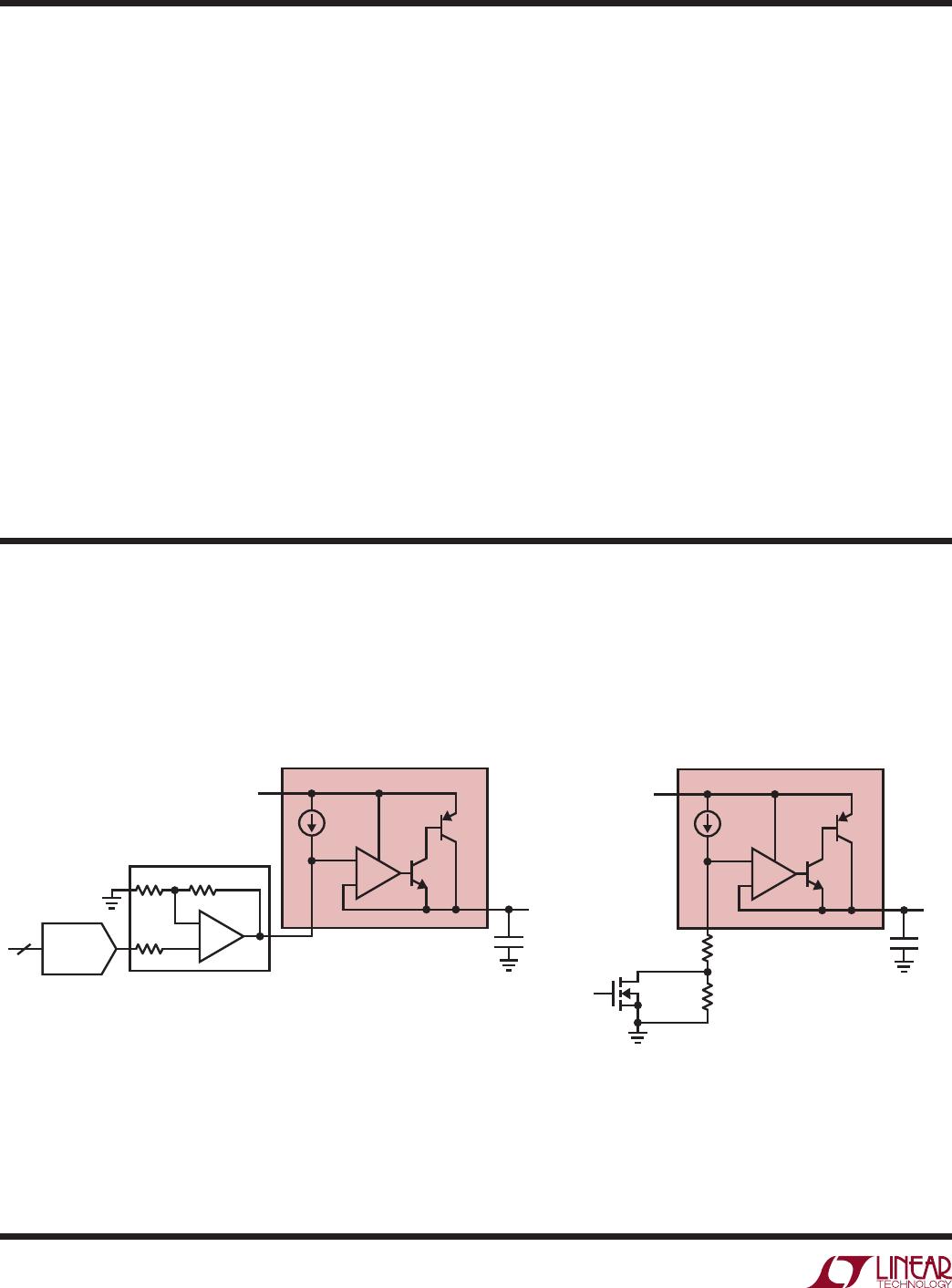
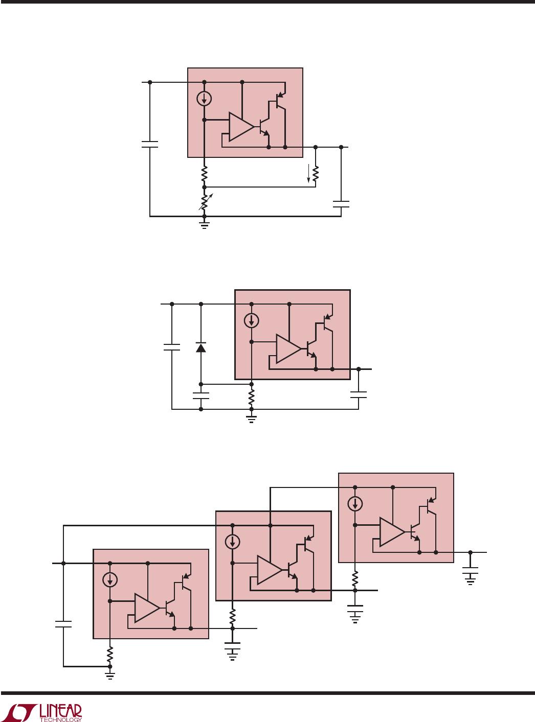
APPLICATIONS INFORMATION
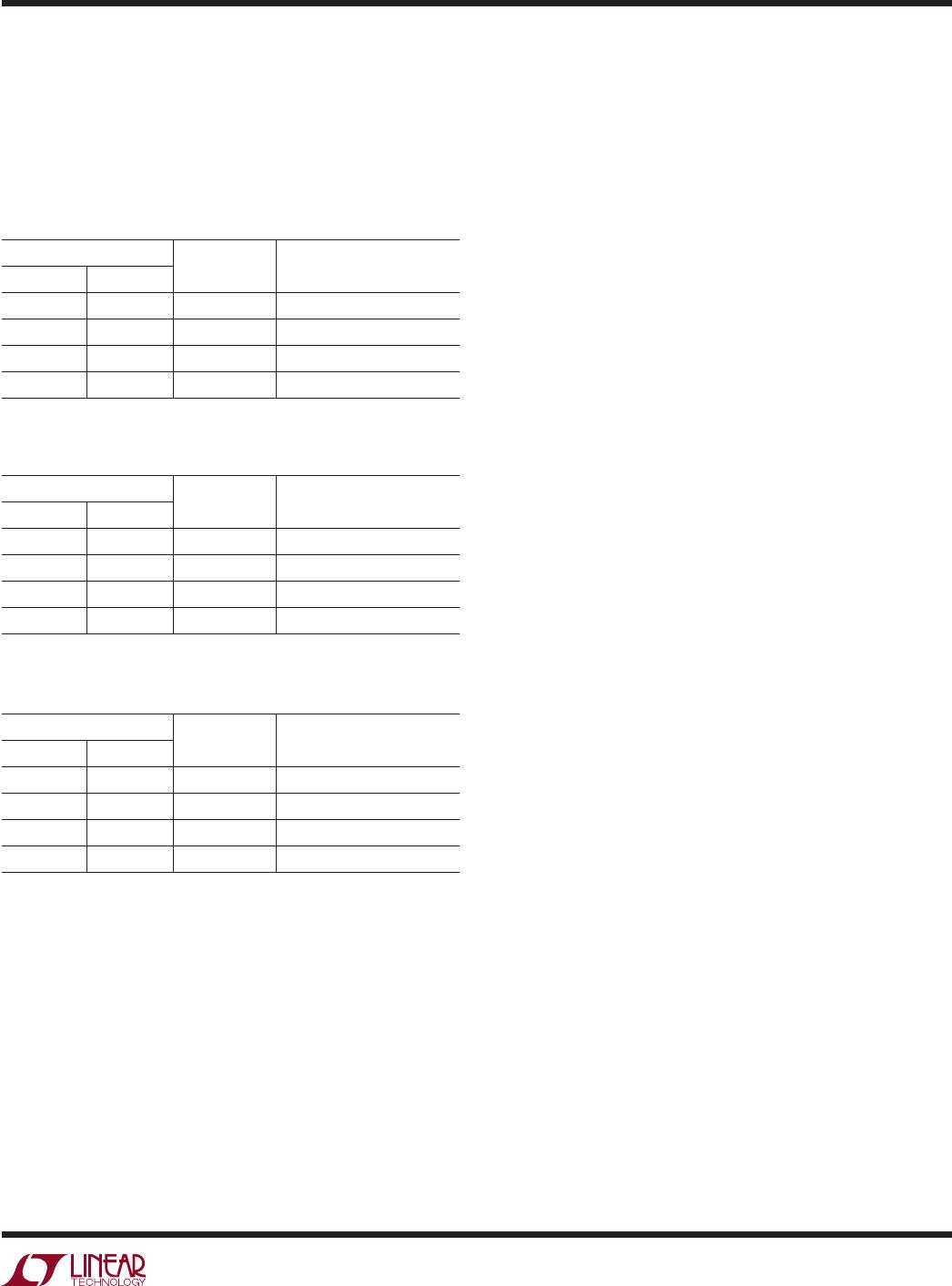
Tables 3 through 5 list thermal resistance as a function
of copper areas in a fi xed board size. All measurements
were taken in still air on a 4-layer FR-4 board with 1oz
solid internal planes and 2oz external trace planes with a
total fi nished board thickness of 1.6mm.
Table 3. DD Package, 8-Lead DFN
COPPER AREA
THERMAL RESISTANCE
(JUNCTION-TO-AMBIENT)
TOPSIDE* BACKSIDE BOARD AREA
2500mm
2
2500mm
2
2500mm
2
25°C/W
1000mm
2
2500mm
2
2500mm
2
25°C/W
225mm
2
2500mm
2
2500mm
2
28°C/W
100mm
2
2500mm
2
2500mm
2
32°C/W
*Device is mounted on topside
Table 4. TS8 Package, 8-Lead SOT-23
COPPER AREA
THERMAL RESISTANCE
(JUNCTION-TO-AMBIENT)
TOPSIDE* BACKSIDE BOARD AREA
2500mm
2
2500mm
2
2500mm
2
54°C/W
1000mm
2
2500mm
2
2500mm
2
54°C/W
225mm
2
2500mm
2
2500mm
2
57°C/W
100mm
2
2500mm
2
2500mm
2
63°C/W
*Device is mounted on topside
Table 5. ST Package, 3-Lead SOT-223
COPPER AREA
THERMAL RESISTANCE
(JUNCTION-TO-AMBIENT)
TOPSIDE* BACKSIDE BOARD AREA
2500mm
2
2500mm
2
2500mm
2
20°C/W
1000mm
2
2500mm
2
2500mm
2
20°C/W
225mm
2
2500mm
2
2500mm
2
24°C/W
100mm
2
2500mm
2
2500mm
2
29°C/W
*Device is mounted on topside
For further information on thermal resistance and using thermal information,
refer to JEDEC standard JESD51, notably JESD51-12.
PCB layers, copper weight, board layout and thermal vias
affect the resultant thermal resistance. Please reference
JEDEC standard JESD51-7 for further information on high
thermal conductivity test boards. Achieving low thermal
resistance necessitates attention to detail and careful layout.
Demo circuit 1447A’s board layout using multiple inner
V
OUT
planes and multiple thermal vias achieves 28°C/W
performance for the DFN package.
Calculating Junction Temperature
Example: Given an industrial factory application with an
input voltage of 15V ±10%, an output voltage of 12V ±5%,
an output current of 200mA and a maximum ambient
temperature of 50°C, what would be the maximum junc-
tion temperature for a DFN package?
The total circuit power equals:
P
TOTAL
= (V
IN
– V
OUT
)(I
OUT
)
The SET pin current is negligible and can be ignored.
V
IN(MAX CONTINUOUS)
= 16.5 (15V + 10%)
V
OUT(MIN CONTINUOUS)
= 11.4V (12V – 5%)
I
OUT
= 200mA
Power dissipation under these conditions equals:
P
TOTAL
= (16.5 – 11.4V)(200mA) = 1.02W
Junction temperature equals:
T
J
= T
A
+ P
TOTAL
• θ
JA
T
J
= 50°C + (1.02W • 30°C/W) = 80.6°C
In this example, junction temperature is below the maxi-
mum rating, ensuring reliable operation.