PDF: 09005aef82b21119/Source: 09005aef82b2112c Micron Technology, Inc., reserves the right to change products or specifications without notice.
JTF8c128_256x64AY.fm - Rev. B 6/08 EN
4 ©2007 Micron Technology, Inc. All rights reserved
1GB, 2GB (x64, SR) 240-Pin DDR3 SDRAM UDIMM
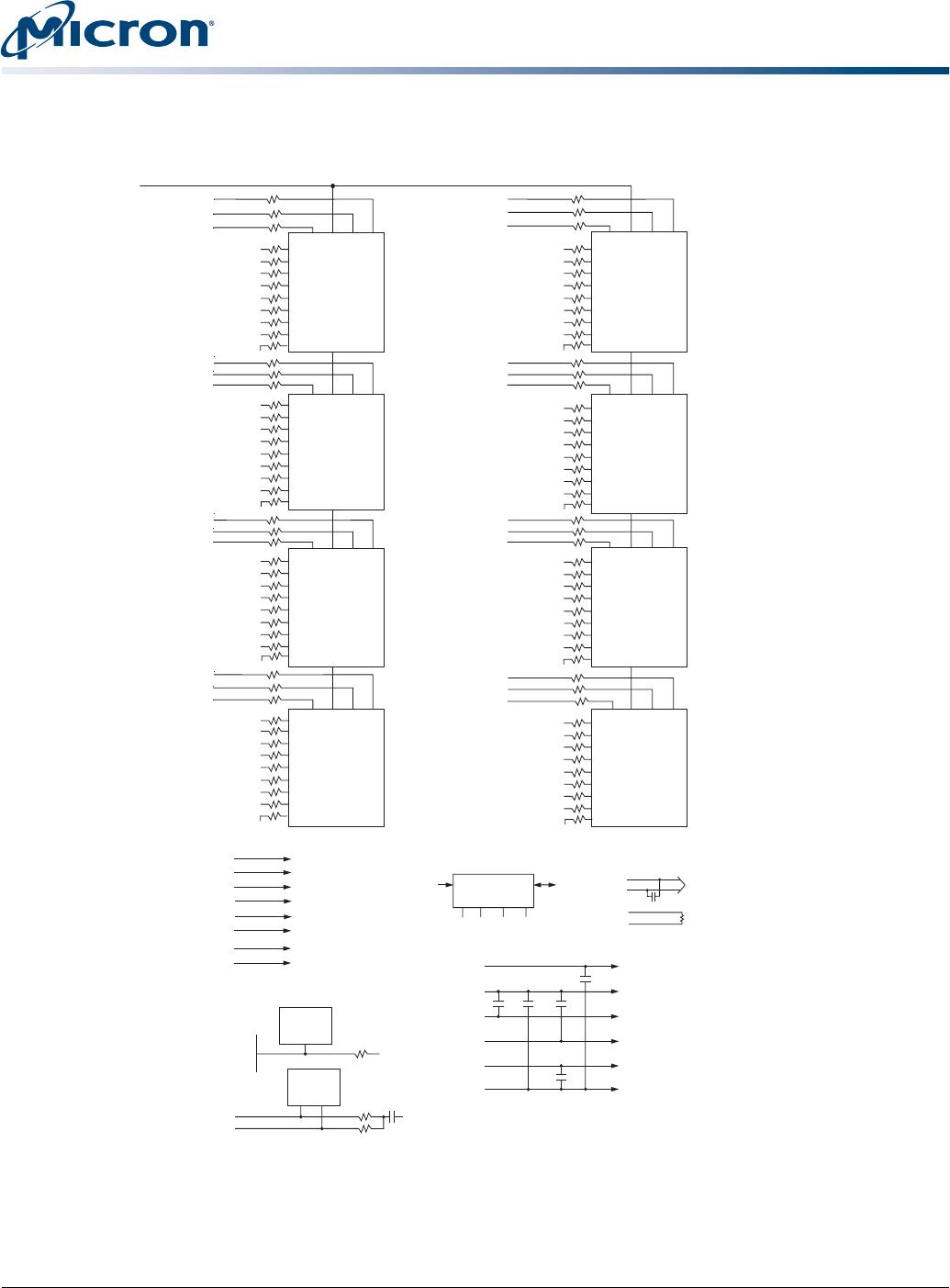
Pin Assignments and Descriptions
Table 6: Pin Descriptions
Symbol Type Description
A[14:0] Input Address inputs: Provide the row address for ACTIVATE commands, and the column address and
auto precharge bit for READ/WRITE commands, to select one location out of the memory array in
the respective bank. A10 is sampled during a PRECHARGE command to determine whether the
PRECHARGE applies to one bank (A10 LOW) or all banks (A10 HIGH). If only one bank is to be
precharged, the bank is selected by BA. A12 is also used for BC4/BL8 identification as “BL on-the-fly”
during CAS commands.. The address inputs also provide the op-code during the mode register
command set
. A[13:0] (1GB), A[14:0] (2GB).
BA[2:0] Input Bank address inputs: BA[2:0] define the device bank to which an ACTIVATE, READ, WRITE, or
PRECHARGE command is being applied. BA[2:0] define which mode register, including MR, EMR,
EMR(2), and EMR(3), is loaded during the LOAD MODE command.
CK[1:0],
CK0#[1:0]
Input Clock: CK0 and CK0# are differential clock inputs. All contorl, command, and address input signals
are sampled on the crossing of the positive edge of CK and the negative edge of CK#. Output data
(DQ and DQS/DQS#) is referenced to the crossings of CK and CK#. CK1, CK1# are terminated.
CKE0 Input Clock enable: CKE (registered HIGH) activates and CKE (registered LOW) deactivates clocking
circuitry on the DDR3 SDRAM.
DM[7:0] Input Input data mask: DM is an input mask signal for write data. Input data is masked when DM is
sampled HIGH, along with that input data, during a write access. DM is sampled on both edges of
DQS. Although DM pins are input-only, the DM loading is designed to match that of the DQ and DQS
pins.
ODT0 Input On-die termination: ODT (registered HIGH) enables termination resistance internal to the DDR3
SDRAM. When enabled, ODT is only applied to the following pins: DQ, DQS,DQS#, and DM. The ODT
input will be ignored if disabled via the LOAD MODE command.
RAS#, CAS#,
WE#
Input Command inputs: RAS#, CAS#, and WE# (along with S#) define the command being entered.
RESET# Input Reset: RESET# is an active LOW CMOS input referenced to V
SS. The RESET# input receiver is a CMOS
input and is defined as a rail-to-rail signal with DC HIGH ≥ 0.8 x V
DD and DC LOW ≤ 0.2 x VDD. RESET#
assertion and desertion are asynchronous.
SA[2:0] Input Presence-detect address inputs: These pins are used to configure the SPD EEPROM address range.
SCL Input Serial clock for presence-detect: SCL is used to synchronize presence-detect data transfer to
and from the module.
S0# Input Chip select: S# enables (registered LOW) and disables (registered HIGH) the command decoder.
With both inputs HIGH, all outputs of the register(s) are disabled except for CKE and ODT. CKE, ODT
and chip select remain in previous state when both outputs are high.
DQ[63:0] I/O Data input/output: Bidirectional data bus.
DQS[7:0],
DQS#[7:0]
I/O Data strobe: Output with read data. Input with write data for source-synchronous operation. Edge-
aligned with read data. Center-aligned with write data. DQS# is only used when the differential
data strobe mode is enabled via the LOAD MODE command.
SDA I/O Serial presence-detect data: SDA is a bidirectional pin used to transfer addresses and data into
and out of the SPD EEPROM on the module.
V
DD Supply Power supply: 1.5V ±0.075V.
VDDSPD Supply Serial EEPROM positive power supply: +3.0V to +3.6V.
V
REFDQ Supply Reference voltage: DQ, DM (VDD/2).
V
REFCA Supply Reference voltage: Control, command, and address (VDD/2).
V
SS Supply Ground.
V
TT Supply Termination voltage: Used for control, command, and address (VDD/2).
NC – No connect: These pins are not connected on the module.