PDF: 09005aef82b21119/Source: 09005aef82b2112c Micron Technology, Inc., reserves the right to change products or specifications without notice.
JTF8c128_256x64AY.fm - Rev. B 6/08 EN
9 ©2007 Micron Technology, Inc. All rights reserved
1GB, 2GB (x64, SR) 240-Pin DDR3 SDRAM UDIMM
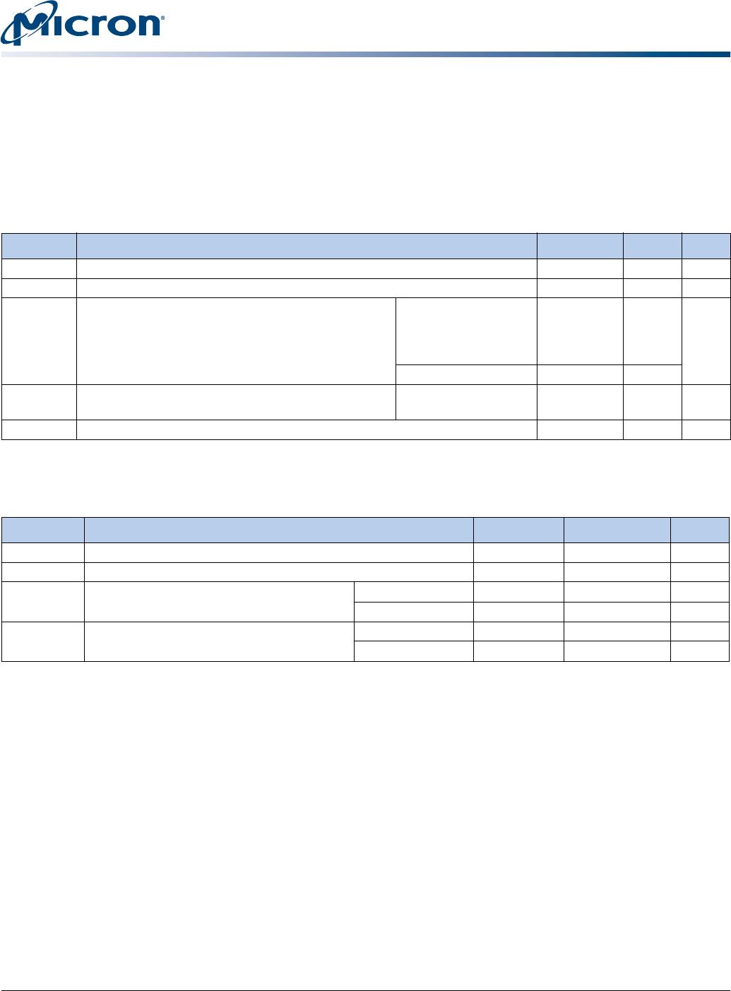
Electrical Specifications
IDD Specifications
Table 10: DDR3 IDD Specifications and Conditions – 1GB
Values are for the MT41J128M8 DDR3 SDRAM only and are computed from values specified in the
1Gb (128 Meg x 8) component data sheet
Parameter Symbol 1333 1066 800 Units
Operating current 0: One bank ACTIVATE-to-PRECHARGE IDD0 880 800 720 mA
Operating current 1: One bank ACTIVATE-to-READ-to-PRECHARGE I
DD1 1,040 960 880 mA
Precharge power-down current: Slow exit IDD2P 80 80 80 mA
Precharge power-down current: Fast exit I
DD2P 200 200 200 mA
Precharge quiet standby current I
DD2Q 400 360 320 mA
Precharge standby current IDD2N 440 400 360 mA
Active power-down current I
DD3P 280 240 200 mA
Active standby current I
DD3N 480 440 400 mA
Burst read operating current IDD4R 1,600 1,280 1,040 mA
Burst write operating current I
DD4W 1,520 1,280 1,040 mA
Refresh current I
DD5B 1,920 1,760 1,600 mA
Self refresh temperature current: MAX T
C
= 85°C IDD6484848mA
Self refresh temperature current (SRT-enabled): MAX T
C
= 95°C IDD6ET 72 72 72 mA
All banks interleaved read current I
DD7 3,920 3,120 2,800 mA
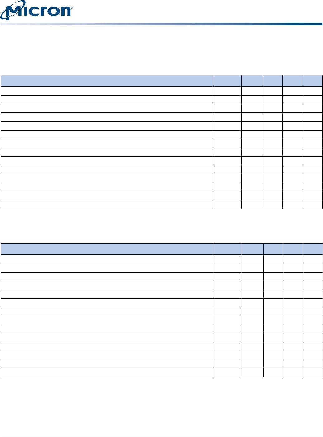
Table 11: DDR3 IDD Specifications and Conditions – 2GB
Values are for the MT41J256M8 DDR3 SDRAM only and are computed from values specified in the
2Gb (256 Meg x 8) component data sheet
Parameter Symbol 1333 1066 800 Units
Operating current 0: One bank ACTIVATE-to-PRECHARGE IDD0 1,040 960 800 mA
Operating current 1: One bank ACTIVATE-to-READ-to-PRECHARGE I
DD1 1,240 1,080 920 mA
Precharge power-down current: Slow exit IDD2P 80 80 80 mA
Precharge power-down current: Fast exit I
DD2P 200 200 200 mA
Precharge quiet standby current I
DD2Q 560 480 400 mA
Precharge standby current I
DD2N 560 480 400 mA
Active power-down current I
DD3P 480 400 360 mA
Active standby current I
DD3N 720 600 520 mA
Burst read operating current IDD4R 2,040 1,800 1,560 mA
Burst write operating current I
DD4W 2,400 2,120 1,840 mA
Refresh current I
DD5B 2,440 2,320 2,200 mA
Self refresh temperature current: MAX T
C
= 85°C IDD6727272mA
Self refresh temperature current (SRT-enabled): MAX T
C
= 95°C IDD6ET 96 96 96 mA
All banks interleaved read current I
DD7 3,680 3,440 3,200 mA