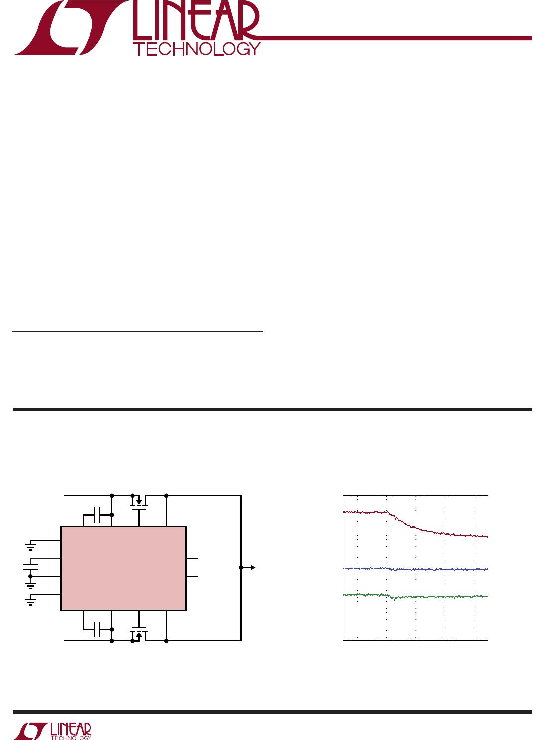
LTC4353
1
4353f
Typical applicaTion
FeaTures DescripTion
Dual Low Voltage
Ideal Diode Controller
The LT C
®
4353 controls external N-channel MOSFETs to
implement an ideal diode function. It replaces two high
power Schottky diodes and their associated heat sinks,
saving power and board area. The ideal diode function
permits low loss power supply ORing and supply holdup
applications.
The LTC4353 regulates the forward-voltage drop across
the MOSFET to ensure smooth current transfer in diode-OR
applications. A fast turn-on reduces the load voltage
droop during supply switchover. If the input supply fails
or is shorted, a fast turn-off minimizes reverse-current
transients.
The controller operates with supplies from 2.9V to 18V. If
both supplies are below 2.9V, an external supply is needed
at the V
CC
pin. Enable inputs can be used to turn off the
MOSFET and put the controller in a low current state.
Status outputs indicate whether the MOSFETs are on or off.
2.9V to 18V, 10A Ideal Diode-OR Output Maintained with Failing Input Supply
applicaTions
n
Low Loss Replacement for Power Diodes
n
Controls N-Channel MOSFETs
n
0V to 18V Supply ORing or Holdup
n
s Gate Turn-On and Turn-Off Time
n
Enable Inputs
n
MOSFET On-Status Outputs
n
16-Lead MSOP and DFN (4mm × 3mm) Packages
n
Redundant Power Supplies
n
Supply Holdup
n
High Availability Systems and Servers
n
Telecom and Network Infrastructure
L, LT , LT C , LT M , Linear Technology and the Linear logo are registered trademarks and
Hot Swap, PowerPath and ThinSOT are trademarks of Linear Technology Corporation. All other
trademarks are the property of their respective owners. Protected by U.S. Patents, including
7920013 and 8022679.
Si4126DY
Si4126DY
GATE1CPO1
CPO2
GND
EN1
EN2
4353 TA01a
2.9V TO 18V
2.9V TO 18V
*OPTIONAL FOR FAST TURN-ON
0.1µF
V
OUT
10A
56nF*
56nF*
V
IN1
V
CC
ONST1
ONST2
OUT1
OUT2
MOSFET
ON-STATUS
OUTPUTS
GATE2
V
IN2
LTC4353
5µs/DIV
VOLTAGE 2V/DIV
4353 TA01b
V
IN1
= 5.2V
V
IN2
= 5V
I
L
= 8A
C
L
= 100µF
V
IN1
V
IN2
V
OUT
LTC4353
2
4353f
absoluTe MaxiMuM raTings
V
IN1
, V
IN2
, OUT1, OUT2 Voltages ...................−2V to 24V
V
CC
Voltage ............................................... 0.3V to 6.5V
GATE1, GATE2 Voltages (Note 3) ............... 0.3V to 34V
CPO1, CPO2 Voltages (Note 3) ................... 0.3V to 34V
EN1, EN2, ONST1, ONST2 Voltages .............0.3V to 24V
CPO1, CPO2 Average Current ................................. 10mA
ONST1, ONST2 Currents ...........................................5mA
(Notes 1, 2)
orDer inForMaTion
LEAD FREE FINISH TAPE AND REEL PART MARKING* PACKAGE DESCRIPTION TEMPERATURE RANGE
LTC4353CDE#PBF LTC4353CDE#TRPBF 4353
16-Pin (4mm × 3mm) Plastic DFN
0°C to 70°C
LTC4353IDE#PBF LTC4353IDE#TRPBF 4353
16-Pin (4mm × 3mm) Plastic DFN
–40°C to 85°C
LTC4353CMS#PBF LTC4353CMS#TRPBF 4353 16-Pin Plastic MSOP 0°C to 70°C
LTC4353IMS#PBF LTC4353IMS#TRPBF 4353 16-Pin Plastic MSOP –40°C to 85°C
Consult LTC Marketing for parts specified with wider operating temperature ranges. *The temperature grade is identified by a label on the shipping container.
For more information on lead free part marking, go to: http://www.linear.com/leadfree/
For more information on tape and reel specifications, go to: http://www.linear.com/tapeandreel/
16
15
14
13
12
11
10
9
17
1
2
3
4
5
6
7
8
EN1
GND
V
CC
V
IN1
GATE1
CPO1
OUT1
ONST1
EN2
NC
NC
V
IN2
GATE2
CPO2
OUT2
ONST2
TOP VIEW
DE PACKAGE
16-LEAD (4mm × 3mm) PLASTIC DFN
T
JMAX
= 125°C, θ
JA
= 43°C/W
EXPOSED PAD (PIN 17) PCB GND CONNECTION OPTIONAL
1
2
3
4
5
6
7
8
EN2
NC
NC
V
IN2
GATE2
CPO2
OUT2
ONST2
16
15
14
13
12
11
10
9
EN1
GND
V
CC
V
IN1
GATE1
CPO1
OUT1
ONST1
TOP VIEW
MS PACKAGE
16-LEAD PLASTIC MSOP
T
JMAX
= 125°C, θ
JA
= 125°C/W
pin conFiguraTion
Operating Ambient Temperature Range
LTC4353C ................................................ C to 70°C
LTC4353I .............................................40°C to 8C
Storage Temperature Range .................. 6C to 150°C
Lead Temperature (Soldering, 10 sec)
MS Package ......................................................300°C
LTC4353
3
4353f
elecTrical characTerisTics
Note 1: Stresses beyond those listed under Absolute Maximum Ratings
may cause permanent damage to the device. Exposure to any Absolute
Maximum Rating condition for extended periods may affect device
reliability and lifetime.
Note 2: All currents into device pins are positive; all currents out of device
pins are negative. All voltages are referenced to GND unless otherwise
specified.
SYMBOL PARAMETER CONDITIONS MIN TYP MAX UNITS
Supplies
V
IN
V
IN1
, V
IN2
Operating Range
With External V
CC
Supply
l
l
2.9
0
18
V
CC
V
V
V
CC(EXT)
V
CC
External Supply Operating Range V
IN1
, V
IN2
≤ V
CC
l
2.9 6 V
V
CC(REG)
V
CC
Regulated Voltage
l
4.5 5 5.5 V
I
IN
V
IN1
, V
IN2
Current
Enabled, Higher Supply
Enabled, Lower Supply
Pull-Up
Disabled
Other V
IN
= 11.7V, Both EN = 0V
Other V
IN
= 12.3V, Both EN = 0V
Both V
IN
= 0V, V
CC
= 5V, Both EN = 0V
Both EN = 1V
l
l
l
l
1.5
200
–45
75
2.5
300
–80
160
mA
µA
µA
µA
I
CC
V
CC
Current
Enabled
Disabled
V
CC
= 5V, Both V
IN
= 1.2V, Both EN = 0V
V
CC
= 5V, Both V
IN
= 1.2V, Both EN = 1V
l
l
1.5
88
2.2
190
mA
µA
V
CC(UVLO)
V
CC
Undervoltage Lockout Threshold V
CC
Rising
l
2.3 2.55 2.7 V
ΔV
CC(HYST)
V
CC
Undervoltage Lockout Hysteresis
l
40 120 300 mV
Ideal Diode Control
V
FR
Forward Regulation Voltage (V
IN
− OUT) V
IN
= 1.2V, V
CC
= 5V
V
IN
= 12V
l
l
2
2
12
25
25
50
mV
mV
ΔV
GATE
MOSFET Gate Drive (GATE – V
IN
) V
FWD
= 0.2V; I = 0, −1μA; Highest V
IN
=12V
V
FWD
= 0.2V; I = 0, −1μA; Highest V
IN
=2.9V
l
l
10
4.5
12
7
14
9
V
V
t
ON(GATE)
GATE1, GATE2 Turn-On Propagation Delay V
FWD
(= V
IN
– OUT) Step: −0.3V to 0.3V
l
0.4 1 µs
t
OFF(GATE)
GATE1, GATE2 Turn-Off Propagation Delay V
FWD
Step: 0.3V to −0.3V
l
0.3 1 µs
I
GATE
GATE1, GATE2 Fast Pull-Up Current
GATE1, GATE2 Fast Pull-Down Current
GATE1, GATE2 Off Pull-Down Current
V
FWD
= 0.4V, ΔV
GATE
= 0V, CPO = 17V
V
FWD
= −0.8V, ΔV
GATE
= 5V
Corresponding EN = 1V, ΔV
GATE
= 2.5V
l
l
l
–0.9
0.9
65
–1.4
1.4
110
–1.9
1.9
160
A
A
µA
Input/Output Pins
V
EN(TH)
EN1, EN2 Threshold Voltage EN Falling
l
580 600 620 mV
ΔV
EN(TH)
EN1, EN2 Threshold Hysteresis
l
2 8 20 mV
I
EN
EN1, EN2 Current At 0.6V
l
0 ±1 µA
I
OUT
OUT1, OUT2 Current
Enabled
Disabled
OUT
n
= 0V, 12V; Both EN = 0V
Both EN = 1V
l
l
–4
8
160
16
µA
µA
I
CPO(UP)
CPO1, CPO2 Pull-Up Current CPO = V
IN
l
–40 –70 –115 µA
V
OL
ONST1, ONST2 Output Low Voltage I = 1mA
I = 3mA
l
l
0.14
0.42
0.4
1.2
V
V
V
OH
ONST1, ONST2 Output High Voltage I = −1μA
l
V
CC
– 1.4 V
CC
– 0.9 V
CC
– 0.5 V
I
ONST
ONST1, ONST2 Leakage Current At 12V
l
0 ±1 µA
ΔV
GATE(ON)
MOSFET On-Detect Threshold (GATE – V
IN
) ONST Pulls Low
l
0.28 0.7 1.1 V
The l denotes those specifications which apply over the full operating
temperature range, otherwise specifications are at T
A
= 25°C. V
IN1
= V
IN2
= 12V, OUT = V
IN
, V
CC
Open, unless otherwise noted.
Note 3: Internal clamps limit the GATE and CPO pins to a minimum of 10V
above, and a diode below the corresponding V
IN
pin. Driving these pins to
voltages beyond the clamp may damage the device.

LTC4353IDE#PBF

Mfr. #:
Manufacturer:
Analog Devices Inc.
Description:
Power Management Specialized - PMIC 2x L V Ideal Diode Cntr
Lifecycle:
New from this manufacturer.
Delivery:
DHL FedEx Ups TNT EMS
Payment:
T/T Paypal Visa MoneyGram Western Union