LTC4353
5
4353f
T
A
= 25°C, V
IN1
= V
IN2
= 12V, OUT = V
IN
, V
CC
open,
unless otherwise noted.
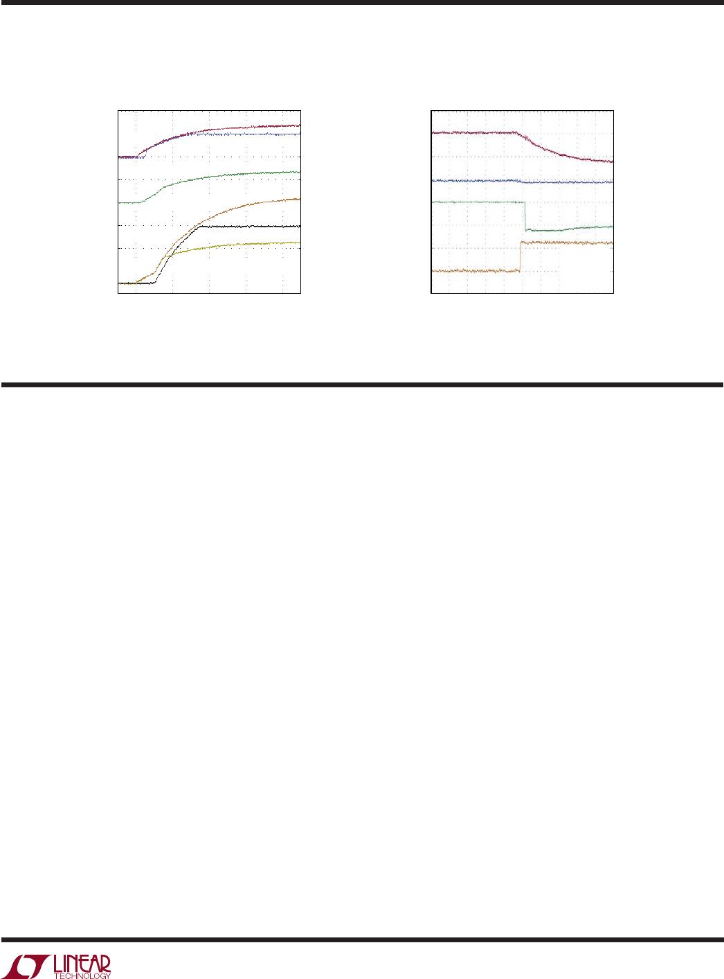
Typical perForMance characTerisTics
Start-Up Waveform on V
IN1
Power-Up
Fast Gate Switchover
From Failing Supply
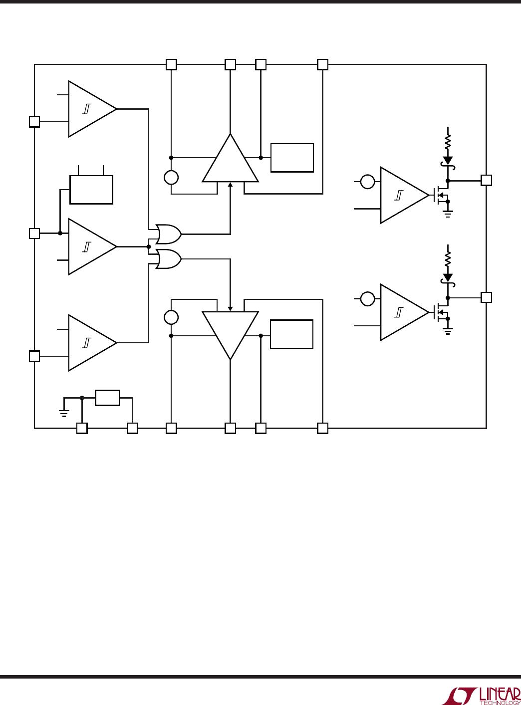
pin FuncTions
CPO1, CPO2: Charge Pump Output. Connect a capacitor
from this pin to the corresponding V
IN
pin. The value of
this capacitor should be approximately 10× the gate ca-
pacitance (C
ISS
) of the MOSFET switch. The charge stored
on this capacitor is used to pull-up the gate during a fast
turn-on. Leave this pin open if fast turn-on is not needed.
EN1, EN2: Enable Input. Keep this pin below 0.6V to en-
able diode control on the corresponding supply. Driving
this pin high shuts off the MOSFET gate (current can still
flow through its body diode). The comparator has a built-in
hysteresis of 8mV. Having both EN pins high lowers the
current consumption of the controller.
Exposed Pad (DE Package Only): This pin may be left
open or connected to device ground.
GATE1, GATE2: MOSFET Gate Drive Output. Connect this
pin to the gate of the external N-channel MOSFET switch.
An internal clamp limits the gate voltage to 12V above,
and a diode below the input supply. During fast turn-on, a
1.4A pull-up current charges GATE from CPO. During fast
turn-off, a 1.4A pull-down current discharges
GATE to V
IN
.
GND: Device Ground.
ONST1, ONST2: MOSFET Status Output. This pin is pulled
low by an internal switch when GATE is more than 0.7V
above V
IN
to indicate an on MOSFET. An internal 500k
resistor pulls this pin up to a diode below V
CC
. It may be
pulled above V
CC
using an external pull-up. Tie to GND or
leave open if unused.
OUT1, OUT2: Output Voltage Sense Input. Connect this
pin to the load side of the MOSFET. The voltage sensed
at this pin is used to control the MOSFET gate.
V
CC
: Low Voltage Supply. Connect a 0.1μF capacitor from
this pin to ground. For V
IN
≥ 2.9V, this pin provides decou-
pling for an internal regulator that generates a 5V supply.
For applications where both V
IN
< 2.9V, also connect an
external supply voltage in the 2.9V to 6V range to this pin.
V
IN1
, V
IN2
: Voltage Sense and Supply Input. Connect
this pin to the supply side of the MOSFET. The low volt-
age supply V
CC
is generated from the higher of V
IN1
and
V
IN2
. The voltage sensed at this pin is used to control the
MOSFET gate.
5ms/DIV
VOLTAGE 5V/DIV
4353 G10
V
IN1
V
CC
OUT
CPO1
CPO2
GATE1
5µs/DIV
4353 G11
∆V
GATE2
10V/DIV
∆V
GATE1
5V/DIV
V
IN2
2V/DIV
V
IN1
2V/DIV
V
IN1
= 5.2V
V
IN2
= 5V
C
L
= 100µF
I
L
= 8A