LTC4353
7
4353f
operaTion
The LTC4353 controls N-channel MOSFETs to emulate
two ideal diodes. When enabled, each servo amplifier
(SA1, SA2) controls the gate of the external MOSFET to
servo its forward voltage drop (V
FWD
= V
IN
OUT) to V
FR
.
The gate voltage rises to enhance the MOSFET if the load
current causes the drop to exceed V
FR
. For large output
currents, the MOSFET gate is driven fully on and the volt-
age drop is equal to I
FET
R
DS(ON)
.
In the case of an input supply short-circuit, when the
MOSFET is conducting, a large reverse current starts
flowing from the load towards the input. SA detects this
failure condition as soon as it appears, and turns off the
MOSFET by rapidly pulling down its gate.
SA quickly pulls up the gate whenever it senses a large for-
ward voltage drop. An external capacitor between the CPO
and V
IN
pins is needed for fast gate pull-up. This capacitor
is charged up, at device power-up, by the internal charge
pump. The stored charge is used for the fast gate pull-up.
The GATE pin sources current from the CPO pin and sinks
current to the V
IN
and GND pins. Clamps limit the GATE
and CPO voltages to 12V above and a diode below V
IN
.
Internal switches pull the ONST pins low when the GATE to
V
IN
voltage exceeds 0.7V to indicate that power is passing
through the MOSFET.
LDO is a low dropout regulator that generates a 5V supply
at the V
CC
pin from the highest V
IN
input. When both V
IN
are below 2.9V, an external supply in the 2.9V to 6V range
is required at the V
CC
pin.
V
CC
and EN pin comparators, CP1 to CP3, control power
passage. The MOSFET is held off whenever the EN pin is
above 0.6V, or the V
CC
pin is below 2.55V. A high on both
EN pins lowers the current consumption of the device.
LTC4353
8
4353f
High availability systems often employ parallel connected
power supplies or battery feeds to achieve redundancy
and enhance system reliability. ORing diodes have been
a popular means of connecting these supplies at the point
of load. Diodes followed by storage capacitors also hold
up supply voltages when an input voltage sags or has a
brownout. The disadvantage of these approaches is the
diode’s significant forward-voltage drop and the result-
ing power loss. The LTC4353 solves these problems by
using an external N-channel MOSFET as the pass element
(see Figure 1). The MOSFET is turned on when power is
being passed, allowing for a low voltage drop from the
supply to the load. When the input source voltage drops
below the output common supply voltage it turns off the
MOSFET, thereby matching the function and performance
of an ideal diode.
applicaTions inForMaTion
Figure 1. 12V Ideal Diode-OR with Status Lights
Figure 2. Power Supply Configurations
Power Supply Configuration
The LTC4353 can operate with input supplies down to 0V.
This requires powering the V
CC
pin with an early external
supply in the 2.9V to 6V range. In this range of operation
V
IN
should be lower than V
CC
. If V
CC
powers up after
V
IN
and backfeeding of V
CC
by the internal 5V LDO is a
concern, then a series resistor (few 100Ω) or Schottky
diode limits device power dissipation and backfeeding of
a low V
CC
supply when any V
IN
is high. A 0.1µF bypass
capacitor should also be connected between the V
CC
and
GND pins, close to the device. Figure 2 illustrates this.
If either V
IN
operates above 2.9V, the external supply at
V
CC
is not needed. The 0.1µF capacitor is still required
for bypassing.
GATE1
4353 F02
0V TO V
CC
0V TO
V
CC
V
IN1
V
CC
GATE2
V
IN2
LTC4353
2.9V TO 6V
GATE1
M1
M2
M1
M2
2.9V TO 18V
(0V TO 18V)
0V TO 18V
(2.9V TO 18V)
V
IN1
V
CC
GATE2
V
IN2
LTC4353
C
VCC
0.1µF
C
VCC
0.1µF
OPTIONAL
OR
HERE
M1
Si4126DY
M2
Si4126DY
GATE1CPO1
CPO2
GND
EN1
EN2
4353 F01
12V
12V
D1, D2: GREEN LED LN1351C
C
VCC
0.1µF
OUT
10A
C1
56nF
R1
2.7k
C2
56nF
V
IN1
V
CC
ONST1
ONST2
OUT1
OUT2
D1
D2
GATE2
V
IN2
LTC4353
R2
2.7k
C
L
LTC4353
9
4353f
MOSFET Selection
The LTC4353 drives N-channel MOSFETs to conduct the
load current. The important features of the MOSFET are
its maximum drain-source voltage BV
DSS
, maximum gate-
source voltage V
GS(MAX)
, and the on-resistance R
DS(ON)
.
If an input is connected to ground, the full supply voltage
can appear across the MOSFET. To survive this, the BV
DSS
must be higher than the supply voltages. The V
GS(MAX)
rating of the MOSFET should exceed 14V since that is
the upper limit of the internal GATE to V
IN
clamp. The
R
DS(ON)
of the MOSFET dictates the maximum voltage drop
(I
L
R
DS(ON)
) and the power dissipated (I
L
2
R
DS(ON)
)
in the MOSFET. Note that the minimum MOSFET voltage
drop is controlled by the servo amplifier regulation volt-
age, hence, picking a very low R
DS(ON)
(below V
FR
/I
L
) may
not be beneficial.
CPO Capacitor Selection
The recommended value of the capacitor between the CPO
and V
IN
pins is approximately 10× the input capacitance
C
ISS
of the MOSFET. A larger capacitor takes a cor-
respondingly longer time to be charged by the internal
charge pump. A smaller
capacitor suffers more voltage
drop
during a fast gate turn-on event as it shares charge
with the MOSFET gate capacitance.
External CPO Supply
The internal charge pump takes milliseconds to charge
up the CPO capacitor especially during device power-up.
This time can be shortened by connecting an external
supply to the CPO pin. A series resistor is needed to limit
the current into the internal clamp between CPO and V
IN
pins. The CPO supply should also be higher than the
main input supply to meet the gate drive requirements
of the MOSFET. Figure 3 shows such a 3.3V ideal diode
application, where a 12V supply is connected to the CPO
pins through a 1k resistor. The 1k limits the current into
the CPO pin, when the V
IN
pin is grounded. For the 8.7V
gate drive (12V – 3.3V), logic-level MOSFETs would be an
appropriate choice for M1 and M2.
Input Transient Protection
When the capacitances at the input and output are very
small, rapid changes in current can cause transients that
exceed the 24V absolute maximum rating of the V
IN
and
OUT pins. In ORing applications, one surge suppressor
connected from OUT to ground clamps all the inputs.
In
the
absence of a surge suppressor, an output capacitance
of 10μF is sufficient in most applications to prevent the
transient from exceeding 24V.
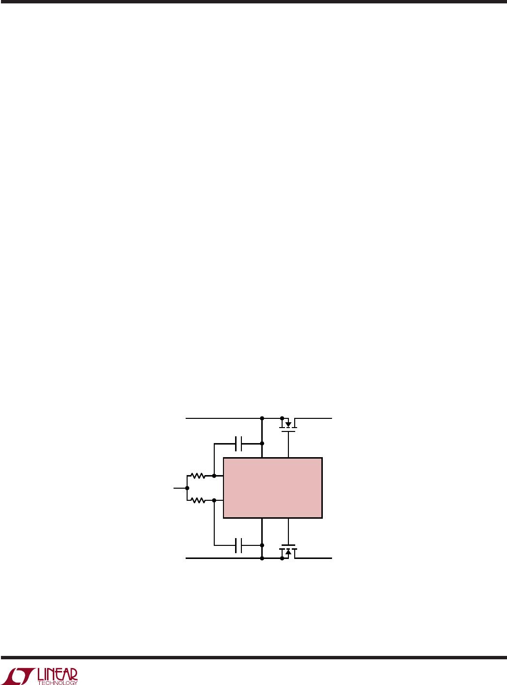
Figure 3. 3.3V Ideal Diode with External 12V Supply
Powering CPO for Faster Start-Up and Refresh
M1
M2
GATE1
4353 F03
V
INA
3.3V
V
INB
3.3V
V
IN1
GATE2
V
IN2
LTC4353
CPO1
CPO2
12V
1k
1k
C1
56nF
C2
56nF
applicaTions inForMaTion

LTC4353IDE#PBF

Mfr. #:
Manufacturer:
Analog Devices Inc.
Description:
Power Management Specialized - PMIC 2x L V Ideal Diode Cntr
Lifecycle:
New from this manufacturer.
Delivery:
DHL FedEx Ups TNT EMS
Payment:
T/T Paypal Visa MoneyGram Western Union