LTC4353
10
4353f
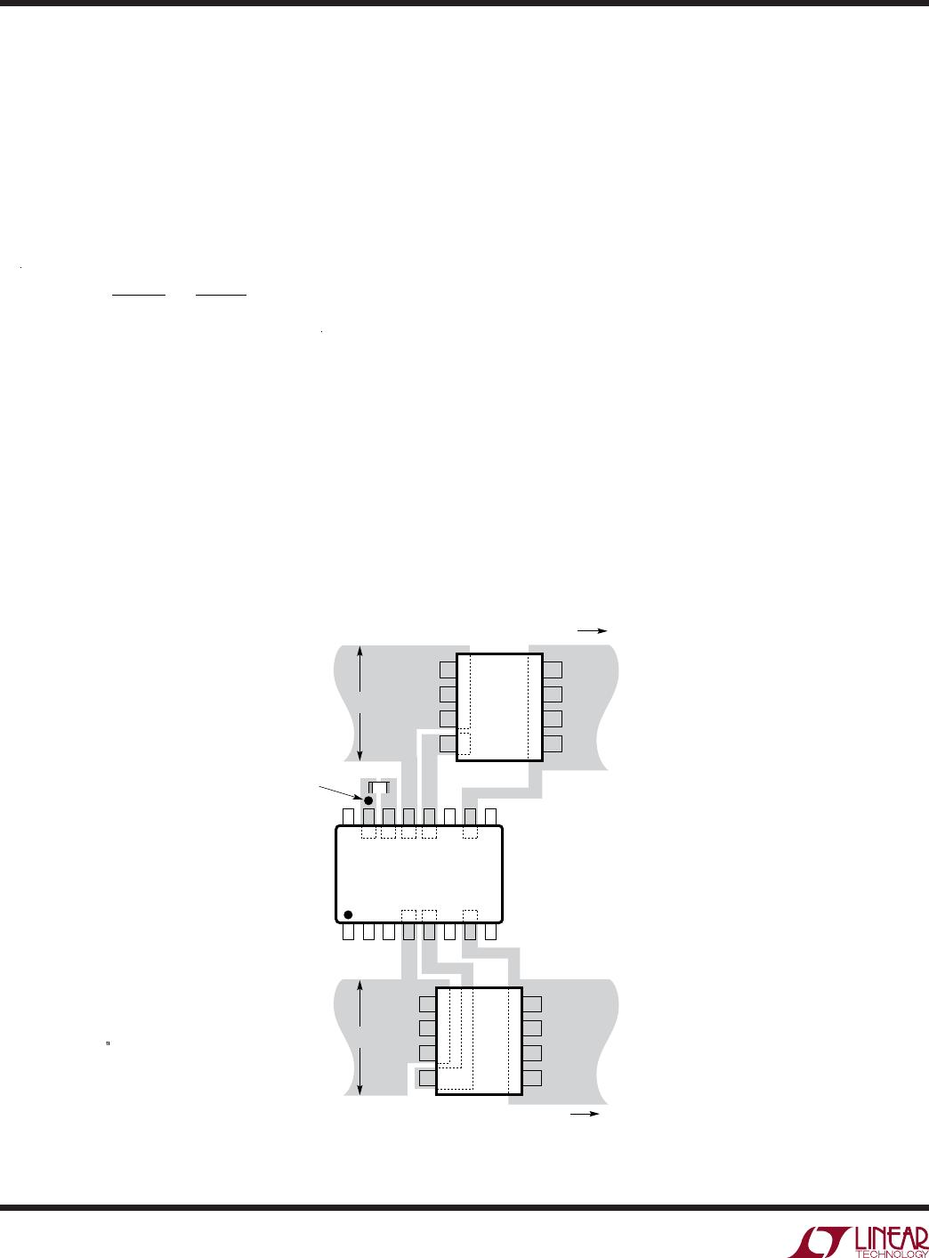
Figure 4. Recommended PCB Layout for M1, M2, C
VCC
applicaTions inForMaTion
Design Example
The following design example demonstrates the calcula-
tions involved for selecting components in a 12V system
with 10A maximum load current (see Figure 1).
First, calculate the R
DS(ON)
of the MOSFET to achieve
the desired forward drop at full load. Assuming a V
DROP
of 30mV:
R
DS(ON)
≤
DROP
I
LOAD
=
30mV
10A
= 3mΩ
The Si4126DY offers a good solution in a SO-8 sized
package with a 2.8mΩ maximum R
DS(ON)
, 30V BV
DSS
,
and 20V V
GS(MAX)
. The maximum power dissipation in
the MOSFET is:
P = I
2
LOAD
• R
DS(ON)
= (10A)
2
• 2.8mΩ = 0.3W
With a maximum steady-state thermal resistance θ
JA
of 35°C/W, 0.3W causes a modest 11°C rise in junction
temperature of the Si4126DY above the ambient.
The input capacitance, C
ISS
, of the Si4126DY is about
5500pF. Following the 10× recommendation, a 56nF
capacitor is selected for C1 and C2.
LEDs, D1 and D2, require around 3mA for good luminous
intensity. Accounting for a 2V diode drop and 0.6V V
OL
,
R1 and R2 are set to 2.7k.
PCB Layout Considerations
Connect the V
IN
and OUT pin traces as close as possible
to the MOSFET’s terminals. Keep the traces to the MOS-
FET wide and short to minimize resistive losses. The PCB
traces associated with the power path through the MOSFET
should have low resistance (see Figure 4).
It is also important to put C
VCC
, the bypass capacitor for
the V
CC
pin, as close as possible between V
CC
and GND.
Place C1 and C2 near the CPO and V
IN
pins. Surge sup-
pressors, when used, should be mounted close to the
LTC4353 using short lead lengths.
4353 F04
MSOP-16
W
CURRENT
FLOW
VIA TO
GROUND
PLANE
S
S
S
G
D
D
D
D
M2
SO-8
TO
LOAD
FROM
SUPPLY B
W
CURRENT
FLOW
S
S
S
G
D
D
D
D
M1
SO-8
TO
LOAD
FROM
SUPPLY A
C
VCC
TRACK WIDTH
W: 0.03 PER AMPERE
ON 1oz Cu FOIL
DRAWING IS NOT TO SCALE!
LTC4353

