I
DD
Specifications
Table 9: DDR2 I
DD
Specifications and Conditions – 1GB (Die Revision G)
Values shown for MT47H128M8 DDR2 SDRAM only and are computed from values specified in the 1Gb (128 Meg x 8) com-
ponent data sheet
Parameter Symbol -1GA
-80E/
-800 -667 Units
Operating one bank active-precharge current:
t
CK =
t
CK (I
DD
),
t
RC =
t
RC
(I
DD
),
t
RAS =
t
RAS MIN (I
DD
); CKE is HIGH, S# is HIGH between valid commands;
Address bus inputs are switching; Data bus inputs are switching
I
DD0
920 720 680 mA
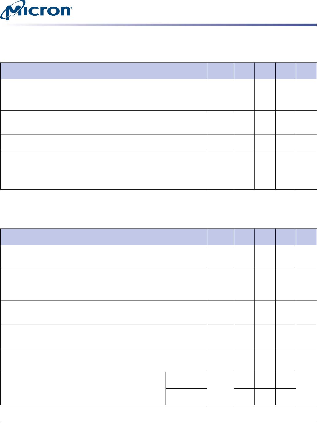
Operating one bank active-read-precharge current: I
OUT
= 0mA; BL = 4, CL
= CL (I
DD
), AL = 0;
t
CK =
t
CK (I
DD
),
t
RC =
t
RC (I
DD
),
t
RAS =
t
RAS MIN (I
DD
),
t
RCD =
t
RCD (I
DD
); CKE is HIGH, S# is HIGH between valid commands; Address bus in-
puts are switching; Data pattern is same as I
DD4W
I
DD1
1040 880 800 mA
Precharge power-down current: All device banks idle;
t
CK =
t
CK (I
DD
); CKE is
LOW; Other control and address bus inputs are stable; Data bus inputs are
floating
I
DD2P
56 56 56 mA
Precharge quiet standby current: All device banks idle;
t
CK =
t
CK (I
DD
); CKE
is HIGH, S# is HIGH; Other control and address bus inputs are stable; Data bus
inputs are floating
I
DD2Q
480 400 320 mA
Precharge standby current: All device banks idle;
t
CK =
t
CK (I
DD
); CKE is
HIGH, S# is HIGH; Other control and address bus inputs are switching; Data bus
inputs are switching
I
DD2N
480 400 320 mA
Active power-down current: All device banks open;
t
CK =
t
CK (I
DD
); CKE is LOW; Other control and address bus inputs are
stable; Data bus inputs are floating
Fast PDN exit
MR[12] = 0
I
DD3P
400 320 240 mA
Slow PDN exit
MR[12] = 1
80 80 80
Active standby current: All device banks open;
t
CK =
t
CK (I
DD
),
t
RAS =
t
RAS
MAX (I
DD
),
t
RP =
t
RP (I
DD
); CKE is HIGH, S# is HIGH between valid commands;
Other control and address bus inputs are switching; Data bus inputs are switch-
ing
I
DD3N
560 480 440 mA
Operating burst write current: All device banks open; Continuous burst
writes; BL = 4, CL = CL (I
DD
), AL = 0;
t
CK =
t
CK (I
DD
),
t
RAS =
t
RAS MAX (I
DD
),
t
RP =
t
RP (I
DD
); CKE is HIGH, S# is HIGH between valid commands; Address bus inputs
are switching; Data bus inputs are switching
I
DD4W
1680 1280 1080 mA
Operating burst read current: All device banks open; Continuous burst read,
I
OUT
= 0mA; BL = 4, CL = CL (I
DD
), AL = 0;
t
CK =
t
CK (I
DD
),
t
RAS =
t
RAS MAX (I
DD
),
t
RP =
t
RP (I
DD
); CKE is HIGH, S# is HIGH between valid commands; Address bus
inputs are switching; Data bus inputs are switching
I
DD4R
1680 1280 1080 mA
Burst refresh current:
t
CK =
t
CK (I
DD
); REFRESH command at every
t
RFC (I
DD
)
interval; CKE is HIGH, S# is HIGH between valid commands; Other control and
address bus inputs are switching; Data bus inputs are switching
I
DD5
2120 1880 1720 mA
Self refresh current: CK and CK# at 0V; CKE ≤ 0.2V; Other control and ad-
dress bus inputs are floating; Data bus inputs are floating
I
DD6
56 56 56 mA
1GB, 2GB (x64, SR) 200-Pin DDR2 SDRAM SODIMM
I
DD
Specifications
PDF: 09005aef83c2a451
htf8c128_256x64hz.pdf - Rev. E 4/14 EN
10
Micron Technology, Inc. reserves the right to change products or specifications without notice.
© 2009 Micron Technology, Inc. All rights reserved.