Si4312
10 Rev. 0.5
3.5. RATIO Selection Used for the Slicer Threshold Calculation Window
In OOK modulation, many different encoding schemes exist, which can result in variable ON and OFF times as
seen in the example data waveforms shown in Figure 4. In order to determine the proper slicer threshold used for
demodulating the OOK signal into digital data, the Si4312 must sample an "ON" and "OFF" event in a time window
called the threshold calculation window. The samples during the "ON" time will determine the ON voltage, and the
samples during the "OFF" time will determine the OFF voltage. These voltages are used to determine the slicer
threshold voltage as follows:
Defining the BT variable from the last section as the ON time and
then, the threshold calculation window is calculated as follows:
The threshold calculation window is 1.25 times longer than the ON plus OFF times for margin to allow sampling of
both ON and OFF times. Figure 5 shows a graph of the threshold calculation window.
Figure 5. Example of the Threshold Calculation
Ratio is a unit-less multiplier that relates the OFF time to the ON time. The Si4312 defines two constants for RATIO
as shown in Table 10 based on the logic level of pin 5.
Table 10. RATIO Constants Based on Logic Level of Pin 5
Pin 5 RATIO
05
110
SlicerThreshold
Max_ON_Voltage Min_OFF_Voltage+
2
-----------------------------------------------------------------------------------------------------------=
RATIO
OFF
ON
------------=
Threshold Calculation Window 1.25 ON OFF+
1.25 BT BT RATIO+
1.25 BT RATIO 1+=
=
=
Threshold Calculation Window
Digital Data
PPM
Encoding
“1” “0” “1” “1”
1000 us
100 us
OOK
Waveform
ON voltage
OFF voltage
Si4312
Rev. 0.5 11
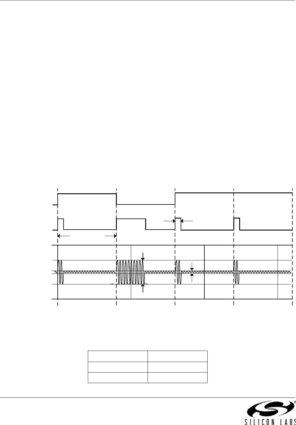
Since the OFF time = RATIO x BT and the values for RATIO are either 5 or 10, RATIO should be chosen such that
either the value of 5 or 10 x the BT[1:0] setting is just larger than the OFF time. For the PPM example shown in
Figure 4, BT[1:0] = (1,1) since BT = 100 µs. The actual OFF time is 900 µs; so, we would set pin 5 = 1 to get a
RATIO of 10 such that the calculated OFF time is BT[1:0] x RATIO = 100 µs x 10 = 1000 µs, which is greater than
the actual OFF time of 900 µs.
An alternative approach to choosing the RATIO bit (pin 5) is to choose the RATIO parameter such that the
threshold calculation window is greater than the actual ON plus OFF times using Table 11 and the values chosen
for BT[1:0].
3.6. Frequency Scanning
The channel bandwidth directly affects the sensitivity of any wireless receiver. Typical analog OOK receivers use
an external ceramic filter with a large bandwidth to accommodate the data rate, crystal tolerances, and transmit
carrier frequency offsets, which leads to unnecessary amounts of noise and lower sensitivity levels. The Si4312
uses a narrow channel bandwidth of 160 kHz and frequency scanning to obtain excellent sensitivity levels
(–110 dBm at data rate of 1 kbps at 315 MHz) while still accommodating up to ±210 kHz of scan bandwidth from its
operating frequency.
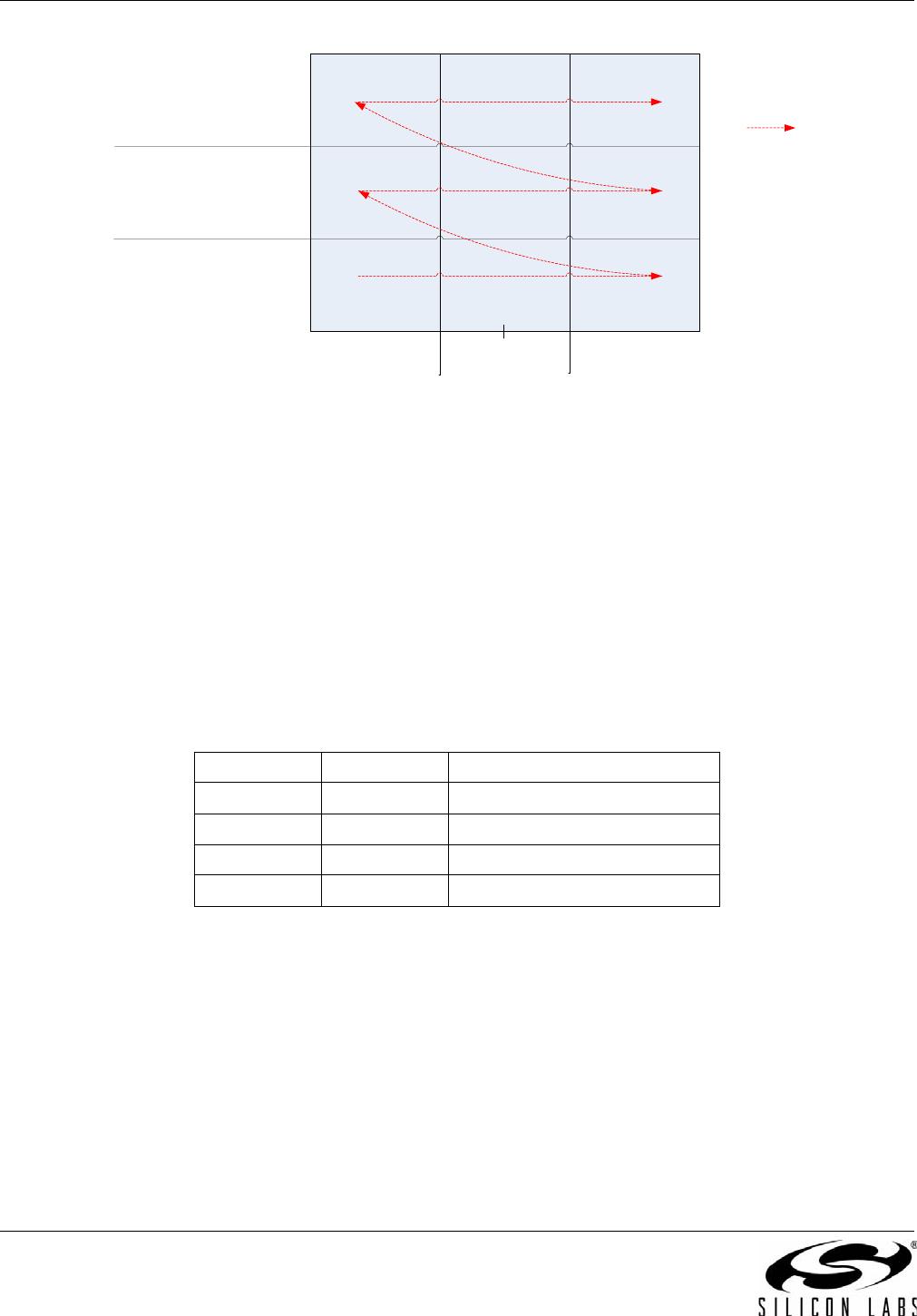
The frequency scan algorithm works by breaking the scan bandwidth (420 kHz) into three frequency bins
approximately 140 kHz wide and checking for transmit signal energy in each bin. Because the received signal
power can vary by large orders of magnitude depending on how close the transmitter is to the receiver, the
frequency algorithm may have to re-scan the frequency bins if the received power level saturates the receiver.
Three gain settings are used in the frequency scan algorithm denoted as high-, medium-, and low-gain.
The chip begins scanning the frequency in the highest receiver gain setting to find signals that have a receive
signal strength indicator (RSSI) level from sensitivity to about –70 dBm. If energy is detected in only one of these
frequency bands, it is double-checked again and deemed as the correct operating frequency band. Therefore, the
frequency scan algorithm takes at least two searches to find the correct frequency band. The scan time per
frequency bin search is equal to the threshold calculation window time as chosen by the RATIO and BT[1:0]
settings given in Table 11. Therefore, the best case frequency scan time is equal to two times the threshold
calculation window time.
In case the input signal is large while the gain is also large, the receiver could be overloaded; therefore, the
frequency scan algorithm follows a series of frequency and gain level settings based on measured RSSI as shown
in Figure 6. In the worst case, there are a total of nine frequency bin searches (three frequency bins times three
gain settings) plus one additional frequency re-scan because we don't know when the signal starts or for double
checking. Thus, the worst-case scan time is equal to 10 times the threshold calculation window time. Figure 6
shows the frequency scan algorithm broken into three frequency bins of 140 kHz and three gain settings.
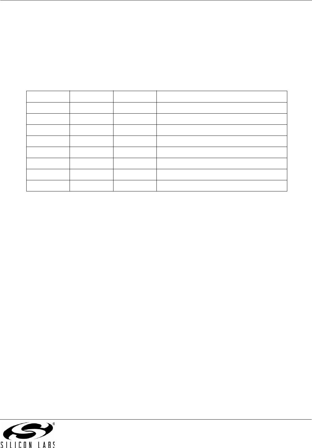
Table 11. Threshold Calculation Window Times Based on RATIO and BT[1:0] Settings
RATIO BT1 BT0 Threshold Calculation Window (ms)
000 7.500
001 3.750
010 1.500
011 0.750
1 0 0 13.750
101 6.875
110 2.750
111 1.375
Si4312
12 Rev. 0.5
Figure 6. Frequency Scan Algorithm Depicting 3 Frequency Bins of 140 kHz and 3 Gain Settings
Frequency scanning is always enabled to find the transmitted signal. The scanning process stops after the correct
frequency band is found for the transmitted signal and is held throughout the duration of the packet plus a time of
no RF signal activity. This dead time is called “threshold hold time” and is described in section 3.7. Theshold hold
time allows a frequency found in the first packet of transmission to be held for any subsequent retransmissions of
packets if the retransmissions occur before the threshold hold time. This held frequency ensures all bits of the
second and subsequent packets are recovered completely. Frequency scanning resumes after the time of no RF
signal activity exceeds the threshold hold time.
3.7. Threshold Hold Time Selection
The threshold hold time is defined as the length of time the Si4312 keeps its slicer threshold voltage level when no
signals are present. If a signal does not appear after this time interval, the Si4312 will re-start the frequency scan
process and look for the signal in one of its three frequency bins. The threshold hold times are determined by the
bit settings chosen on pins 16 and 17 as shown in Table 12.
3.8. Low Noise Amplifier Input Circuit
Figure 2 shows the typical application circuit with 50 matching. Components C3 and L1 are used to transform the
input impedance of the LNA. C3 is equal to 15 pF and L1 is equal to 33 nH at 433.92 MHz and 62 nH at 315 MHz
for 50 matching.
Table 12. Threshold Time Settings Based on TH[1:0] Logic Levels
TH1 (Pin 16) TH0 (Pin 17) Threshold Hold Time (ms)
00 70
01 100
10 300
11 500
Freq Bin 1
Fc
Low Gain:
Input RSSI in the range of
-45dBm ~ -15dBm
Scan
Directions
Medium Gain:
Input RSSI in the range of
-75dBm to -40dBm
High Gain:
Input RSSI in the range of
Sensitivity to -70dBm
Freq Bin 2 Freq Bin 3

SI4312-B10-GMR

Mfr. #:
Manufacturer:
Silicon Labs
Description:
RF Receiver Sub-GHz receiver
Lifecycle:
New from this manufacturer.
Delivery:
DHL FedEx Ups TNT EMS
Payment:
T/T Paypal Visa MoneyGram Western Union

Products related to this Datasheet