Si4312
16 Rev. 0.5
6. Package Markings (Top Marks)
6.1. Si4312 Top Mark
Figure 7. Si4312 Top Mark Example
6.2. Top Mark Explanation
Mark Method: YAG Laser
Line 1 Marking: Part Number 12 = Si4312
Firmware Revision 10 = Firmware Revision 1.0
Line 2 Marking: Die Revision B = Revision B Die
TTT = Internal Code Internal tracking code
Line 3 Marking: Circle = 0.5 mm Diameter
(Bottom-Left Justified)
Pin 1 Identifier
YWW = Date Code Assigned by the Assembly House. Corresponds to the last digit
of the current year (Y) and the workweek (WW) of the mold
date.
1 2 1 0
R T T T
Y W W
Si4312
Rev. 0.5 17
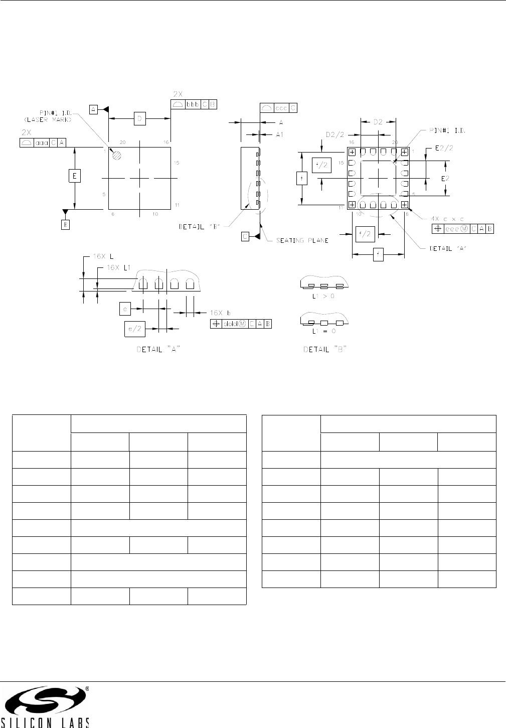
7. Package Outline: Si4312-B10-GM
Figure 8 illustrates the package details for the Si4312-B10-GM. Table 13 lists the values for the dimensions shown
in the illustration.
Figure 8. 20-Pin Quad Flat No-Lead (QFN)
Table 13. Package Dimensions
Symbol Millimeters Symbol Millimeters
Min Nom Max Min Nom Max
A 0.80 0.85 0.90 f 2.53 BSC
A1 0.00 0.02 0.05 L 0.30 0.35 0.40
b 0.20 0.25 0.30 L1 0.00 0.10
c 0.27 0.32 0.37 aaa 0.05
D 3.00 BSC bbb 0.05
D2 1.65 1.70 1.75 ccc 0.08
e 0.50 BSC ddd 0.10
E 3.00 BSC eee 0.10
E2 1.65 1.70 1.75
Notes:
1. All dimensions are shown in millimeters (mm) unless otherwise noted.
2. Dimensioning and tolerancing per ANSI Y14.5M-1994.
Si4312
18 Rev. 0.5
8. PCB Land Pattern: Si4312-B10-GM
Figure 9 illustrates the PCB land pattern details for the Si4312-B10-GM. Table 14 lists the values for the
dimensions shown in the illustration.
Figure 9. PCB Land Pattern

SI4312-B10-GMR

Mfr. #:
Manufacturer:
Silicon Labs
Description:
RF Receiver Sub-GHz receiver
Lifecycle:
New from this manufacturer.
Delivery:
DHL FedEx Ups TNT EMS
Payment:
T/T Paypal Visa MoneyGram Western Union

Products related to this Datasheet