Si4312
8 Rev. 0.5
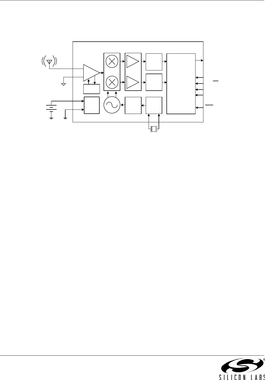
3. Functional Description
3.1. Overview
Figure 3. Functional Block Diagram
The Si4312 is a fully-integrated OOK CMOS RF
receiver that operates in the unlicensed 315 and 433.92
MHz ultra high frequency (UHF) bands. It is designed
for high-volume, cost-sensitive RF receiver applications.
The chip operates at a carrier frequency of 315 or
433.92 MHz and supports OOK digital modulation with
data rates of up to 10 kbps NRZ or 5 kbps Manchester
coded. The Si4312 has selectable data filters to
optimize the sensitivity of the receiver for a given data
rate. The Si4312 employs a frequency scanning
algorithm to improve the sensitivity of the receiver with a
small IF bandwidth while still maintaining the ability to
accommodate large transmit frequency offsets. The
integrated on-chip squelch circuit prevents false output
data when the RF input signal is absent or below
sensitivity.
The device leverages Silicon Labs’ patented and proven
digital low-IF architecture and offers superior sensitivity
and interference rejection. The Si4312 can achieve
superior sensitivity in the presence of large interference
due to its high dynamic range ADCs and digital filters.
The digital low-IF architecture also enables superior
blocking ability and low intermodulation distortion for
robust reception in the presence of wide-band
interference.
Digital integration reduces the number of required
external components compared to traditional offerings,
resulting in a solution that only requires a 16 MHz
crystal and passive components allowing a small and
compact printed circuit board (PCB) implementation
area. The high integration of the Si4312 improves the
system manufacturing reliability, improves quality, eases
design-in, and minimizes costs.
3.2. Receiver Description
The RF input signal is amplified by a low-noise amplifier
(LNA) and down-converts to a low intermediate
frequency with a quadrature image-reject mixer. The
mixer output is amplified by a programmable gain
amplifier (PGA), filtered, and digitized with a high-
resolution analog-to-digital converter (ADC). All RF
functions are integrated into the device eliminating any
production alignment issues associated with external
components, such as SAW and ceramic IF filters.
Silicon Labs’ advanced digital low-IF architecture
achieves superior performance by using the DSP to
perform channel filtering, demodulation, automatic gain
control (AGC), automatic frequency control (AFC), and
other baseband processing. DSP implementation of the
channel filters provides better repeatability and control
of the bandwidth and frequency response of the filter
compared to analog implementations. No off-chip
ceramic filters are needed with the Si4312 as all IF
channel filtering is performed in the digital domain.
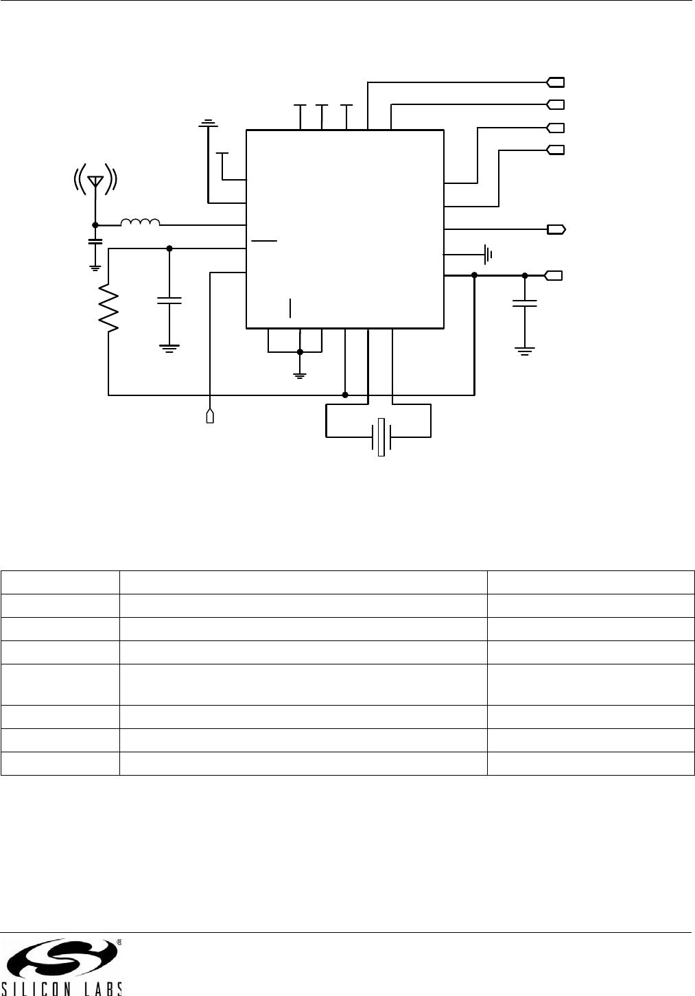
Si4312
RX_IN
AGC
Antenna
LDO
VDD
GND
2.7 – 3.6 V
LNA
XTAL
OSC
RST
RATIO
ADC
ADC
PGA
DSP
MCU
BASEBAND
PROCESSOR
SQUELCH
16 MHz
FREQ
SCAN
315/434
TH[1:0]
DOUT
BT[1:0]