Si4312
6 Rev. 0.5
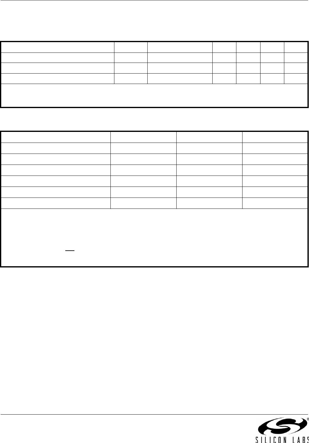
Table 5. Si4312 Receiver Characteristics
(T
A
= 25 °C, V
DD
= 3.3 V, R
s
= 50 Ω, F
RF
= 433.92 MHz unless otherwise noted)
Parameter Symbol Test Condition Min Typ Max Unit
Sensitivity @ BER = 10
–3 (Note 1)
1.0 kbps, 315 MHz
(Note2)
— –110 — dBm
10 kbps, 315 MHz
(Note2)
— –103 — dBm
1.0 kbps, 433.92 MHz
(Note2)
— –106 — dBm
10 kbps, 433.92 MHz TBD –101 — dBm
Data Rate
3
NRZ — — 10 kbps
Adjacent Channel Rejection
±200 kHz
(Note 1)
Desired signal is 3 dB above sensitivity
(BER = 10
–3
), unmodulated interferer
is at ±200 kHz, rejection measured as
difference between desired signal and
interferer level in dB when BER = 10
–3
TBD 35 — dB
Alternate Channel Rejection
±400 kHz
1,2
Desired signal is 3 dB above sensitivity
(BER = 10
–3
), unmodulated interferer
is at ±400 kHz, rejection measured as
difference between desired signal and
interferer level in dB when BER = 10
–3
— 55 — dB
Image Rejection, IF = 128 kHz
1,2
— 23 — dB
Blocking
1,2
±2 MHz, 1.0 kbps, desired signal is
3 dB above sensitivity, CW interferer
level is increased until BER = 10
–3
— 65 — dB
±10 MHz, 1.0 kbps, desired signal is
3 dB above sensitivity, CW interferer
level is increased until BER = 10
–3
— 70 — dB
Maximum RF Input Power
1,2
— 8 — dBm
Input IP3
3
| f
2
–f
1
| = 5 MHz, high gain mode,
desired signal is 3 dB above sensitivity,
CW interference levels are increased
until BER = 10
–3
—–10—dBm
LNA Input Capacitance
3
—7—pF
Receiver Channel Bandwidth
4
—160—kHz
RX Boot Time
3
From reset — 500 — ms
Notes:
1. 1.0 kbps, Manchester encoded, RATIO = 0, TH[1:0] = 00, xtal = ±20 ppm.
2. Guaranteed by characterization.
3. Guaranteed by design.
4. The frequency scanning (see section “3.6. Frequency Scanning”) extends this to 420 kHz.
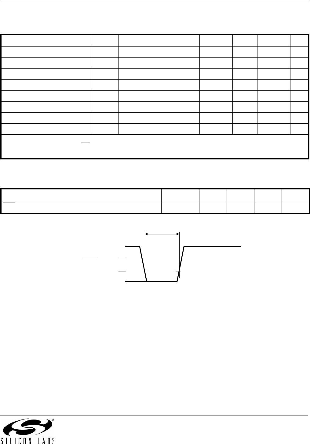
Table 6. Crystal Characteristics
(V
DD
= 3.3 V, T
A
=25°C)
Parameter
Symbol Test Condition Min Typ Max Unit
Crystal Oscillator Frequency — 16 — MHz
Crystal ESR — — 100
XTL1, XTL2 Input Capacitance — 11 — pF