HIGH RIPPLE-REJECTION LOW DROPOUT CMOS VOLTAGE REGULATOR
S-1165 Series
Rev.4.1_02
10
Explanation of Terms
1. Low dropout voltage regulator
This voltage regulator has the low dropout voltage due to its built-in low on-resistance transistor.
2. Output voltage (V
OUT
)
The accuracy of the output voltage is ensured at 1.0% under the specified conditions of fixed input
voltage
*1
, fixed output current, and fixed temperature.
*1. Differs depending the product.
Caution If the above conditions change, the output voltage value may vary and exceed the
accuracy range of the output voltage. Refer to " Electrical Characteristics" and "
Characteristics (Typical Data)" for details.
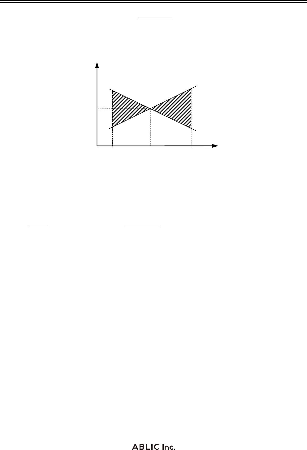
3. Line regulation
V
OUT1
V
IN
V
OUT
Indicates the dependency of the output voltage on the input voltage. That is, the value shows how
much the output voltage changes due to a change in the input voltage with the output current remaining
unchanged.
4. Load regulation (V
OUT2
)
Indicates the dependency of the output voltage on the output current. That is, the value shows how
much the output voltage changes due to a change in the output current with the input voltage remaining
unchanged.
5. Dropout voltage (V
drop
)
Indicates the difference between input voltage (V
IN1
) and the output voltage when; decreasing input
voltage (V
IN
) gradually until the output voltage has dropped out to the value of 98% of output voltage
(V
OUT3
), which is at V
IN
= V
OUT(S)
 1.0 V.
V
drop
V
IN1
 (V
OUT3
0.98)
HIGH RIPPLE-REJECTION LOW DROPOUT CMOS VOLTAGE REGULATOR
Rev.4.1_02
S-1165 Series
11
6. Output voltage temperature coefficient
V
OUT
Ta V
OUT
The shaded area in Figure 10 is the range where V
OUT
varies in the operation temperature range when
the output voltage temperature coefficient is 100 ppm/C.
V
OUT
(
E
)
*1
Example of S-1165B28 typ. product
40
25
0.28 mV/C
V
OUT
[V]
*1. V
OUT(E)
is the value of the output voltage measured at Ta = 25C.
85
Ta [C]
0.28 mV/C
Figure 10
A change in the temperature of the output voltage [mV/°C] is calculated using the following equation.
V
OUT
Ta
[]
mV/°C
*1
= V
OUT(S)
[]
V
*2
V
OUT
Ta V
OUT
[]
ppm/°C
*3
1000
*1. Change in temperature of output voltage
*2. Set output voltage
*3. Output voltage temperature coefficient
HIGH RIPPLE-REJECTION LOW DROPOUT CMOS VOLTAGE REGULATOR
S-1165 Series
Rev.4.1_02
12
Operation
1. Basic operation
Figure 11 shows the block diagram of the S-1165 Series.
The error amplifier compares the reference voltage (V
ref
) with feedback voltage (V
fb
), which is the output
voltage resistance-divided by feedback resistors (R
s
and R
f
). It supplies the gate voltage necessary to
maintain the constant output voltage which is not influenced by the input voltage and temperature
change, to the output transistor.
*1
*1. Parasitic diode
VSS
Current
supply


V
fb
V
ref
VIN
VOUT
R
f
R
s
Error
amplifier
Reference voltage
circuit
Figure 11
2. Output transistor
In the S-1165 Series, a low on-resistance P-channel MOS FET is used as the output transistor.
Be sure that V
OUT
does not exceed V
IN
0.3 V to prevent the voltage regulator from being damaged due
to reverse current flowing from the VOUT pin through a parasitic diode to the VIN pin, when the potential
of V
OUT
became higher than V
IN
.

S-1165B28MC-N6NTFG

Mfr. #:
Manufacturer:
ABLIC
Description:
LDO Voltage Regulators LINEAR LDO REG HI 35UA IQ 200MA IOUT
Lifecycle:
New from this manufacturer.
Delivery:
DHL FedEx Ups TNT EMS
Payment:
T/T Paypal Visa MoneyGram Western Union