HIGH RIPPLE-REJECTION LOW DROPOUT CMOS VOLTAGE REGULATOR
Rev.4.1_02
S-1165 Series
7
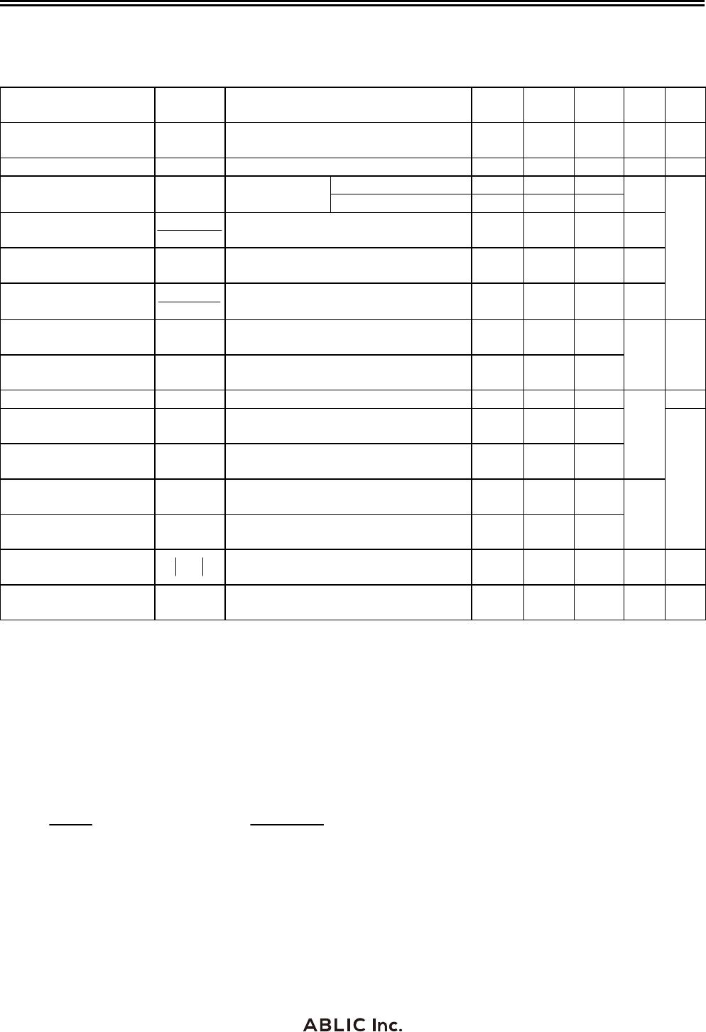
Electrical Characteristics
Table 4
(Ta 25C unless otherwise specified)
Item Symbol Conditions Min. Typ. Max. Unit
Test
Circuit
Output voltage
*1
V
OUT(E)
V
IN
V
OUT(S)
1.0 V, I
OUT
30 mA
V
OUT(S)
0.99
V
OUT(S)
V
OUT(S)
1.01
V 1
Output current
*2
I
OUT
V
IN
V
OUT
S
1.0 V
200
*5
mA 3
Dropout voltage
*3
V
dro
I
OUT
200 mA 1.5 V V
OUT
S
2.5 V 0.20 0.30 V 1
2.6 V V
OUT
S
5.5 V 0.14 0.20
Line regulation
OUTIN
OUT1
VV
V
V
OUT(S)
0.5 V V
IN
6.5 V,
I
OUT
30 mA
0.05 0.2 %/V
Load regulation V
OUT2
V
IN
V
OUT(S)
1.0 V,
1.0 mA I
OUT
200 mA
20 40 mV
Output voltage
temperature coefficient
*4
OUT
OUT
VTa
V
V
IN
V
OUT(S)
1.0 V, I
OUT
30 mA,
40C Ta 85C
100
ppm/
C
Current consumption
during operation
I
SS1
V
IN
V
OUT(S)
1.0 V, ON/OFF pin ON,
no load
35 65 A2
Current consumption
during power-off
I
SS2
V
IN
V
OUT(S)
1.0 V, ON/OFF pin OFF,
no load
0.1 1.0
Input voltage V
IN
2.0 6.5 V
ON/OFF pin
input voltage “H”
V
SH
V
IN
V
OUT(S)
1.0 V, R
L
1.0 k 1.5 4
ON/OFF pin
input voltage “L”
V
SL
V
IN
V
OUT(S)
1.0 V, R
L
1.0 k 0.3
ON/OFF pin
input current “H”
I
SH
V
IN
6.5 V, V
ON/OFF
6.5 V 0.1 0.1 A
ON/OFF pin
input current “L”
I
SL
V
IN
6.5 V, V
ON/OFF
= 0 V 0.1 0.1
Ripple rejection
RR
V
IN
V
OUT(S)
1.0 V, f 1.0 kHz,
V
ri
0.5 Vrms, I
OUT
30 mA
70 dB 5
Short-circuit current I
short
V
IN
V
OUT(S)
1.0 V, ON/OFF pin ON,
V
OUT
0 V
350 mA 3
*1. V
OUT(S)
: Set output voltage
V
OUT(E)
: Actual output voltage
Output voltage when fixing I
OUT
( 30 mA) and inputting V
OUT
S
1.0 V
*2. The output current at which the output voltage becomes 95% of V
OUT(E)
after gradually increasing the output
current.
*3. V
drop
V
IN1
(V
OUT3
0.98)
V
OUT3
is the output voltage when V
IN
V
OUT(S)
1.0 V and I
OUT
200 mA.
V
IN1
is the input voltage at which the output voltage becomes 98% of
V
OUT3
after gradually decreasing
the input voltage.
*4. A change in the temperature of the output voltage [mV/°C] is calculated using the following equation.
V
OUT
Ta
[]
mV/°C
*1
= V
OUT(S)
[]
V
*2
V
OUT
Ta V
OUT
[]
ppm/°C
*3
1000
*1. Change in temperature of output voltage
*2. Set output voltage
*3. Output voltage temperature coefficient
*5. The output current can be at least this value.
Due to restrictions on the package power dissipation, this value may not be satisfied. Attention should be
paid to the power dissipation of the package when the output current is large.
This specification is guaranteed by design.