HIGH RIPPLE-REJECTION LOW DROPOUT CMOS VOLTAGE REGULATOR
Rev.4.1_02
S-1165 Series
13
3. ON/OFF pin
This pin starts and stops the regulator.
When the ON/OFF pin is set to OFF level, the entire internal circuit stops operating, and the built-in P-
channel MOS FET output transistor between the VIN pin and the VOUT pin is turned off, reducing current
consumption significantly. The VOUT pin becomes the Vss level due to the internally divided resistance
of several hundreds k between the VOUT pin and the VSS pin.
The structure of the ON/OFF pin is as shown in Figure 12. Since the ON/OFF pin is neither pulled
down nor pulled up internally, do not use it in the floating status. In addition, note that the current
consumption increases if a voltage of 0.3 V to V
IN
– 0.3 V is applied to the ON/OFF pin. When not using
the ON/OFF pin, connect it to the VSS pin in the product A type, connect it to the VIN pin in B type.
Table 5
Product Type ON/OFF Pin Internal Circuit VOUT Pin Voltage Current Consumption
A “L”: ON Operate Set value I
SS1
A “H”: OFF Stop V
SS
level I
SS2
B “L”: OFF Stop V
SS
level I
SS2
B “H”: ON Operate Set value I
SS1
VSS
ON/OFF
VIN
Figure 12
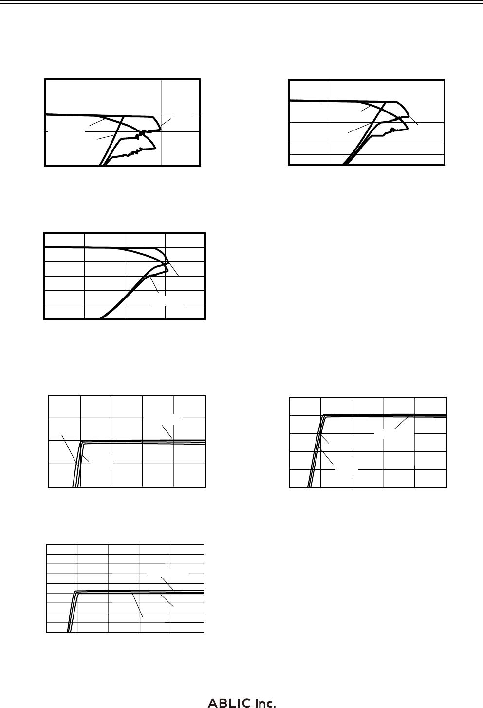
Selection of Output Capacitor (C
L
)
The S-1165 Series performs phase compensation using the internal phase compensator in the IC and the
ESR (Equivalent Series Resistance) of the output capacitor to enable stable operation independent of
changes in the output load. Therefore, always place a capacitor (C
L
) of 2.2 F or more between the
VOUT pin and the VSS pin.
For stable operation of the S-1165 Series, it is essential to employ a capacitor whose ESR is within an
optimum range. Using a capacitor whose ESR is outside the optimum range (approximately 0.5 to
5 ), whether larger or smaller, may cause an unstable output, resulting in oscillation. For this reason, a
tantalum electrolytic capacitor is recommended.
When a ceramic capacitor or an OS capacitor with a low ESR is used, it is necessary to connect an
additional resistor that serves as the ESR in series with the output capacitor. The required resistance
value is approximately 0.5 to 5 , which varies depending on the usage conditions, so perform sufficient
evaluation for selection. Ordinarily, around 1.0 is recommended.
Note that an aluminum electrolytic capacitor may increase the ESR at a low temperature, causing
oscillation. When using this kind of capacitor, perform thorough evaluation, including evaluation of
temperature characteristics.
HIGH RIPPLE-REJECTION LOW DROPOUT CMOS VOLTAGE REGULATOR
S-1165 Series
Rev.4.1_02
14
Precautions
Wiring patterns for the VIN pin, the VOUT pin and GND should be designed so that the impedance is
low. When mounting an output capacitor between the VOUT pin and the VSS pin (C
L
) and a capacitor
for stabilizing the input between the VIN pin and the VSS pin (C
IN
), the distance from the capacitors to
these pins should be as short as possible.
Note that generally the output voltage may increase when a series regulator is used at low load current
(1.0 mA or less).
The S-1165 Series performs phase compensation by using an internal phase compensator and the ESR
of an output capacitor. Therefore, always place a capacitor of 2.2 F or more between VOUT and VSS
pins. A tantalum type capacitor is recommended. Moreover, to secure stable operation of the S-1165
Series, it is necessary to employ a capacitor with an ESR within an optimum range (0.5 to 5 ).
Using a capacitor whose ESR is outside the optimum range (approximately 0.5 to 5 ), whether larger
or smaller, may cause an unstable output, resulting in oscillation. Perform sufficient evaluation under
the actual usage conditions for selection, including evaluation of temperature characteristics.
The voltage regulator may oscillate when the impedance of the power supply is high and the input
capacitance is small or an input capacitor is not connected.
Overshoot may occur in the output voltage momentarily if the voltage is rapidly raised at power-on or
when the power supply fluctuates. Sufficiently evaluate the output voltage at power-on with the actual
device.
The application conditions for the input voltage, the output voltage, and the load current should not
exceed the package power dissipation.
Do not apply an electrostatic discharge to this IC that exceeds the performance ratings of the built-in
electrostatic protection circuit.
In determining the output current, attention should be paid to the output current value specified in Table
4 in “ Electrical Characteristics” and footnote *5 of the table.
ABLIC Inc. claims no responsibility for any disputes arising out of or in connection with any infringement
by products including this IC of patents owned by a third party.
HIGH RIPPLE-REJECTION LOW DROPOUT CMOS VOLTAGE REGULATOR
Rev.4.1_02
S-1165 Series
15
Characteristics (Typical Data)
(1) Output voltage vs. Output current (when load current increases)
S-1165B15 (Ta 25°C) S-1165B30 (Ta 25°C)
VOUT [V]
0
0.5
1
1.5
2
2.5
0 200 400 600 800
V
IN
1.8 V
2.5 V
6.0 V
VOUT [V]
0
0.5
1
1.5
2
2.5
3
3.5
4
0 200 400 600 800
V
IN
= 3.3 V
4.0 V
6.0 V
IOUT [mA]
IOUT [mA]
S-1165B50 (Ta 25°C)
VOUT [V]
0
1
2
3
4
5
6
0 200 400 600 800
V
IN
5.3
V
6.0
V
Remark In determining the output current, attention
should be paid to the following.
1)
The minimum output current value and
footnote *5 of Table 4 in the “ Electrical
Characteristics
2) The package power dissipation
IOUT [mA]
(2) Output voltage vs. Input voltage
S-1165B15 (Ta 25°C) S-1165B30 (Ta 25°C)
VOUT [V]
VOUT [V]
VIN [V]
VIN [V]
S-1165B50 (Ta 25°C)
VOUT [V]
VIN [V]
1 1.5 2 2.5
30 mA
50 mA
I
OUT
= 1mA
1.6
1.55
1.5
1.45
1.4
2.5 3 3.5 4
3.05
3
2.95
2.9
2.85
2.8
30 mA
50 mA
I
OUT
= 1mA
4.5 5 5.5 6
5.1
5.08
5.06
5.04
5.02
5
4.98
4.96
4.94
4.92
30 mA
50 mA
I
OUT
= 1mA

S-1165B28MC-N6NTFG

Mfr. #:
Manufacturer:
ABLIC
Description:
LDO Voltage Regulators LINEAR LDO REG HI 35UA IQ 200MA IOUT
Lifecycle:
New from this manufacturer.
Delivery:
DHL FedEx Ups TNT EMS
Payment:
T/T Paypal Visa MoneyGram Western Union