HIGH RIPPLE-REJECTION LOW DROPOUT CMOS VOLTAGE REGULATOR
S-1165 Series
Rev.4.1_02
4
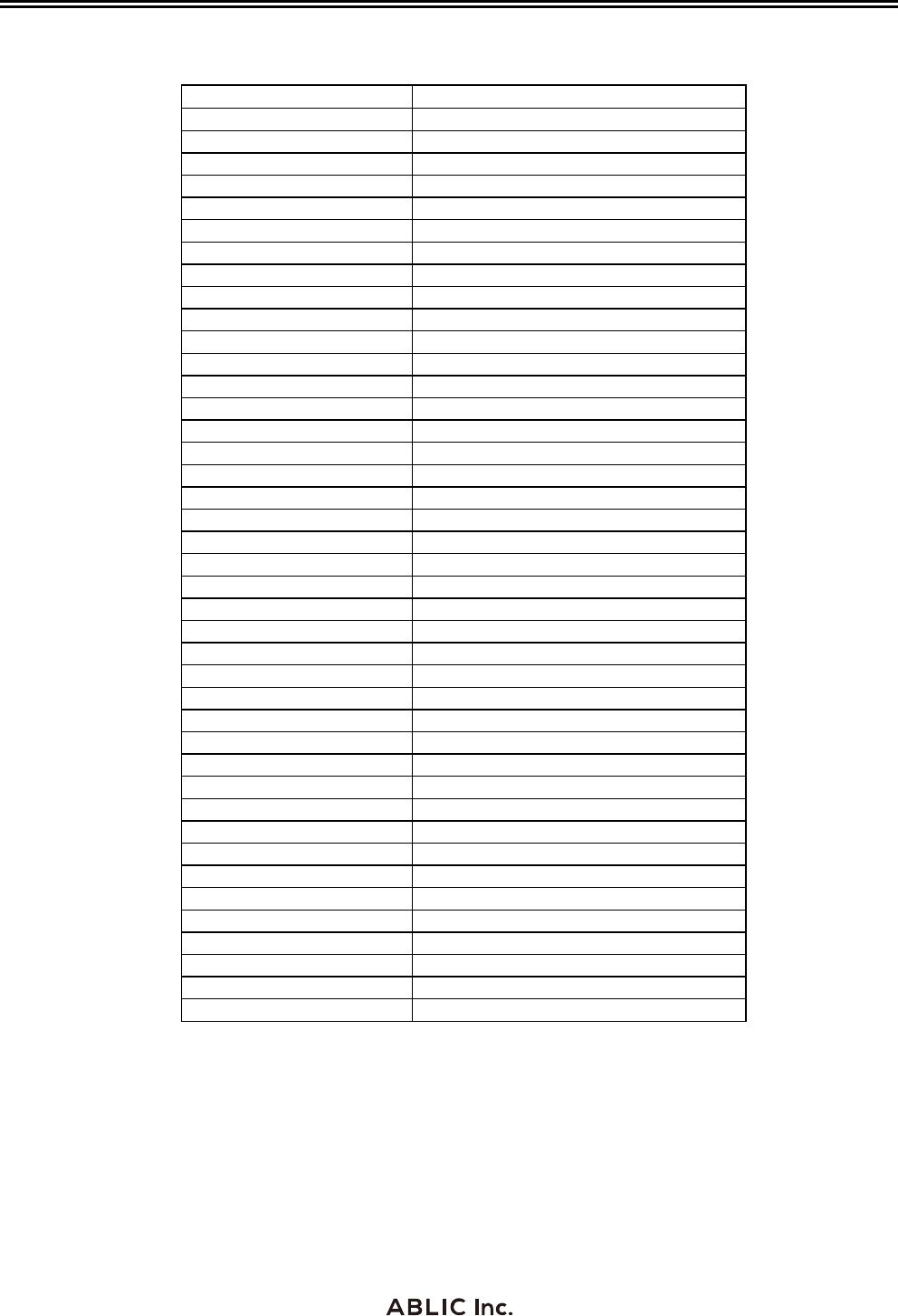
3. Product name list
Table 1
Output Voltage Product Name
1.5V±1.0% S-1165B15MC-N6ATFx
1.6V±1.0% S-1165B16MC-N6BTFx
1.7V±1.0% S-1165B17MC-N6CTFx
1.8V±1.0% S-1165B18MC-N6DTFx
1.9V±1.0% S-1165B19MC-N6ETFx
2.0V±1.0% S-1165B20MC-N6FTFx
2.1V±1.0% S-1165B21MC-N6GTFx
2.2V±1.0% S-1165B22MC-N6HTFx
2.3V±1.0% S-1165B23MC-N6ITFx
2.4V±1.0% S-1165B24MC-N6JTFx
2.5V±1.0% S-1165B25MC-N6KTFx
2.6V±1.0% S-1165B26MC-N6LTFx
2.7V±1.0% S-1165B27MC-N6MTFx
2.8V±1.0% S-1165B28MC-N6NTFx
2.9V±1.0% S-1165B29MC-N6OTFx
3.0V±1.0% S-1165B30MC-N6PTFx
3.1V±1.0% S-1165B31MC-N6QTFx
3.2V±1.0% S-1165B32MC-N6RTFx
3.3V±1.0% S-1165B33MC-N6STFx
3.4V±1.0% S-1165B34MC-N6TTFx
3.5V±1.0% S-1165B35MC-N6UTFx
3.6V±1.0% S-1165B36MC-N6VTFx
3.7V±1.0% S-1165B37MC-N6WTFx
3.8V±1.0% S-1165B38MC-N6XTFx
3.9V±1.0% S-1165B39MC-N6YTFx
4.0V±1.0% S-1165B40MC-N6ZTFx
4.1V±1.0% S-1165B41MC-N7ATFx
4.2V±1.0% S-1165B42MC-N7BTFx
4.3V±1.0% S-1165B43MC-N7CTFx
4.4V±1.0% S-1165B44MC-N7DTFx
4.5V±1.0% S-1165B45MC-N7ETFx
4.6V±1.0% S-1165B46MC-N7FTFx
4.7V±1.0% S-1165B47MC-N7GTFx
4.8V±1.0% S-1165B48MC-N7HTFx
4.9V±1.0% S-1165B49MC-N7ITFx
5.0V±1.0% S-1165B50MC-N7JTFx
5.1V±1.0% S-1165B51MC-N7KTFx
5.2V±1.0% S-1165B52MC-N7LTFx
5.3V±1.0% S-1165B53MC-N7MTFx
5.4V±1.0% S-1165B54MC-N7NTFx
5.5V±1.0% S-1165B55MC-N7OTFx
Remark 1. Please contact our sales office for type A products.
2. x: G or U
3. Please select products of environmental code = U for Sn 100%,
halogen-free products.
HIGH RIPPLE-REJECTION LOW DROPOUT CMOS VOLTAGE REGULATOR
Rev.4.1_02
S-1165 Series
5
Pin Configuration
5 4
1 3 2
SOT-23-5
Top view
Table 2
Pin No. Symbol Description
1 VIN Input voltage pin
2 VSS GND pin
3 ON/OFF ON/OFF pin
4 NC
*1
No connection
5 VOUT Output voltage pin
*1. The NC pin is electrically open.
The NC pin can be connected to VIN pin or VSS pin.
Figure 2
HIGH RIPPLE-REJECTION LOW DROPOUT CMOS VOLTAGE REGULATOR
S-1165 Series
Rev.4.1_02
6
Absolute Maximum Ratings
Table 3
(Ta 25C unless otherwise specified)
Item Symbol Absolute Maximum Rating Unit
Input voltage V
IN
V
SS
0.3 to V
SS
7
V
V
ON/OFF
V
SS
0.3 to V
IN
0.3
Output voltage V
OUT
V
SS
0.3 to V
IN
0.3
Power dissipation P
D
300 (When not mounted on board) mW
600
*1
mW
Operation ambient temperature T
o
pr
40 to 85 C
Storage temperature T
st
g
40 to 125
*1. When mounted on board
[Mounted on board]
(1) Board size : 114.3 mm 76.2 mm t1.6 mm
(2) Board name : JEDEC STANDARD51-7
Caution The absolute maximum ratings are rated values exceeding which the product could suffer
physical damage. These values must therefore not be exceeded under any conditions.
0
50
100 150
600
400
0
Power Dissi
ation
P
D
mW
Ambient Tem
p
erature
(
Ta
)
[
C
]
200
100
300
500
700
Figure 3 Power Dissipation of Package (When Mounted on Board)

S-1165B28MC-N6NTFG

Mfr. #:
Manufacturer:
ABLIC
Description:
LDO Voltage Regulators LINEAR LDO REG HI 35UA IQ 200MA IOUT
Lifecycle:
New from this manufacturer.
Delivery:
DHL FedEx Ups TNT EMS
Payment:
T/T Paypal Visa MoneyGram Western Union