1
LT1995
1995fb
+
4k
4k
+
2k
2k
1k
INPUT
RANGE
–15V TO 15V
1k
4k
LT1995
–15V
1995 TA01a
15V
OUT
REF
M1 M2 M4
P1 P2 P4
4k
, LTC and LT are registered trademarks of Linear Technology Corporation.
All other trademarks are the property of their respective owners.
32MHz, 1000V/µs
Gain Selectable Amplifier
Internal Gain Setting Resistors
Pin Configurable as a Difference Amplifier,
Inverting and Noninverting Amplifier
Difference Amplifier:
Gain Range 1 to 7
CMRR > 65dB
Noninverting Amplifier:
Gain Range 1 to 8
Inverting Amplifier:
Gain Range –1 to –7
Gain Error: <0.2%
Slew Rate: 1000V/µs
Bandwidth: 32MHz (Gain = 1)
Op Amp Input Offset Voltage: 2.5mV Max
Quiescent Current: 9mA Max
Wide Supply Range: ±2.5V to ±15V
Available in 10-Lead MSOP and
10-Lead (3mm × 3mm) DFN Packages
Instrumentation Amplifier
Current Sense Amplifier
Video Difference Amplifier
Automatic Test Equipment
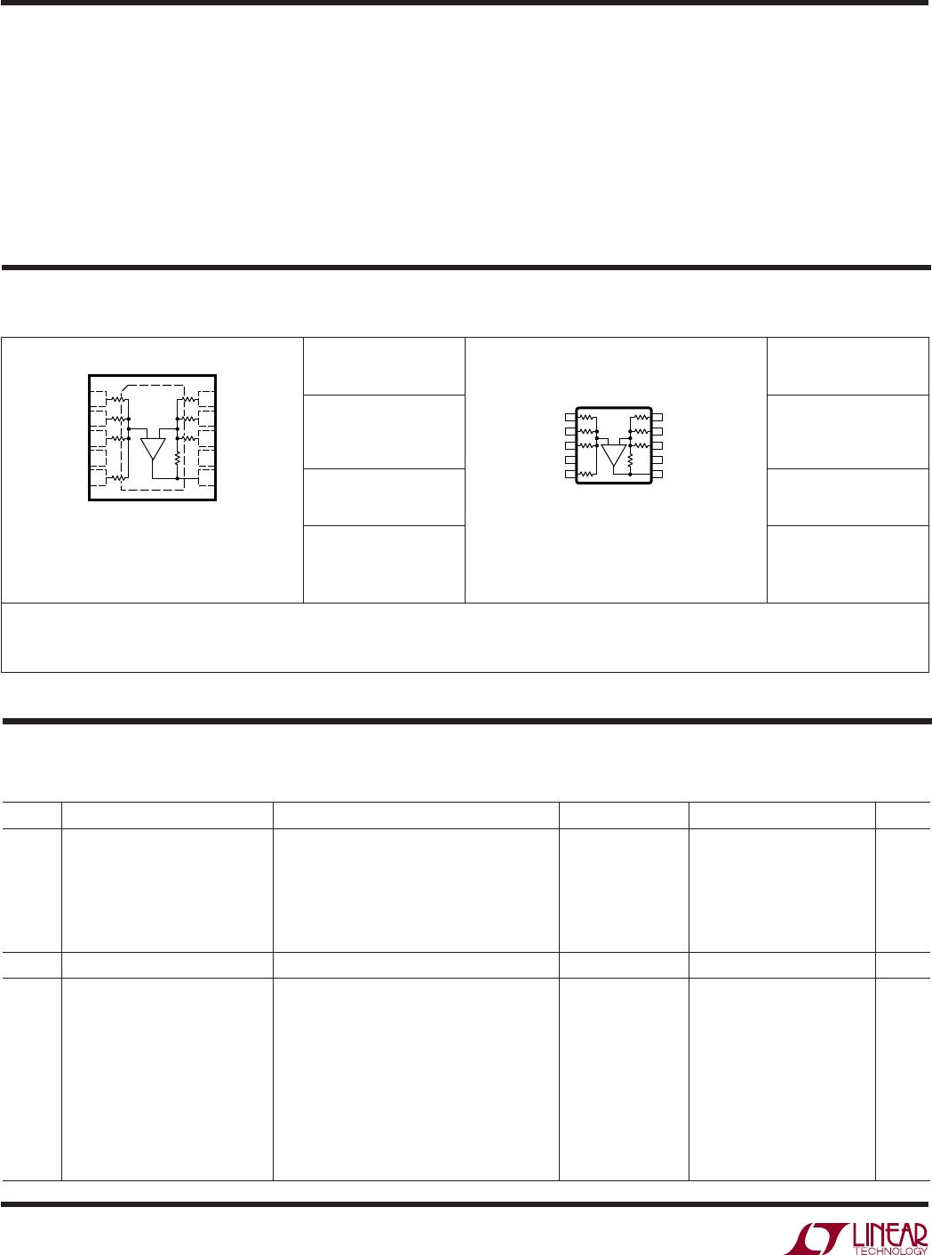
High Slew Rate Differential Gain of 1
FEATURES
APPLICATIO S
U
TYPICAL APPLICATIO
U
DESCRIPTIO
U
The LT
®
1995 is a high speed, high slew rate, gain select-
able amplifier with excellent DC performance. Gains from
–7 to 8 with a gain accuracy of 0.2% can be achieved using
no external components. The device is particularly well
suited for use as a difference amplifier, where the excellent
resistor matching results in a typical common mode
rejection ratio of 79dB.
The amplifier is a single gain stage design similar to the
LT1363 and features superb slewing and settling charac-
teristics. Input offset of the internal operational amplifier
is less than 2.5mV and the slew rate is 1000V/µs. The
output can drive a 150 load to ±2.5V on ±5V supplies,
making it useful in cable driver applications.
The resistors have excellent matching, 0.2% maximum at
room temperature and 0.3% from –40°C to 85°C. The
temperature coefficient of the resistors is typically
–30ppm/°C. The resistors are extremely linear with volt-
age, resulting in a gain nonlinearity of 10ppm.
The LT1995 is fully specified at ±2.5V, ±5V and ±15V sup-
plies and from –40°C to 85°C. The device is available in
space saving 10-lead MSOP and 10-Lead (3mm × 3mm)
DFN packages. For a micropower precision amplifier with
precision resistors, see the LT1991 and LT1996.
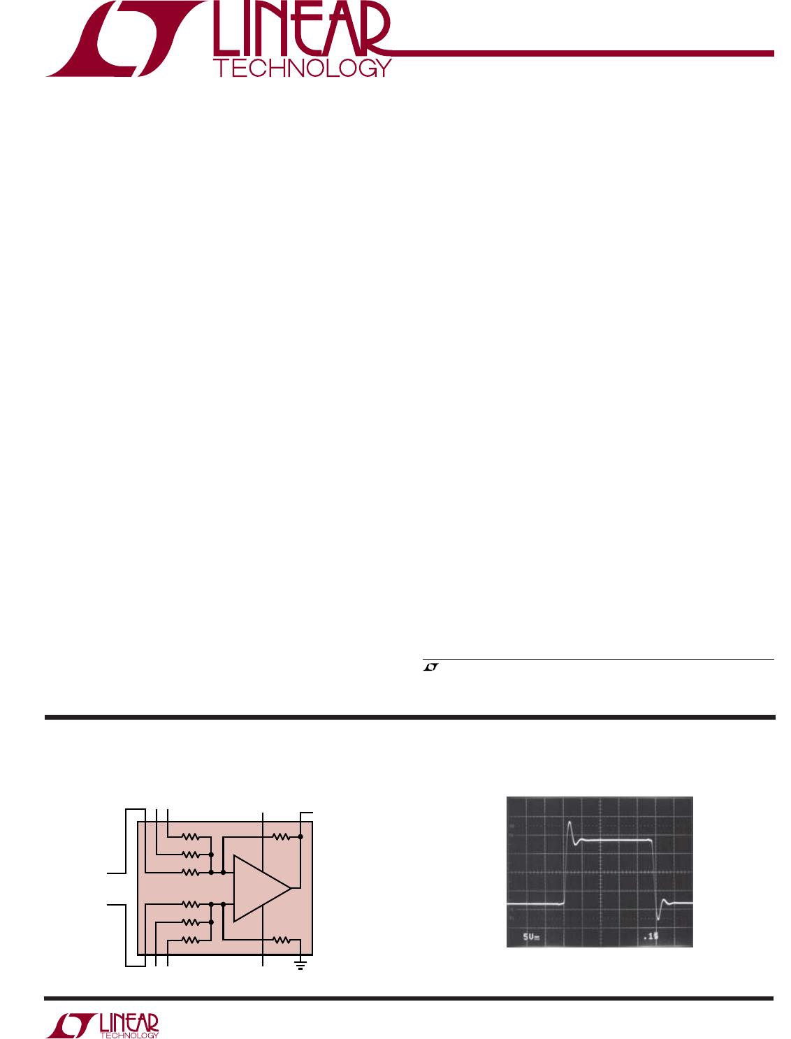
Large-Signal Transient (G = 1)
1995 TA01b
2
LT1995
1995fb
SYMBOL PARAMETER CONDITIONS V
SUPPLY
MIN TYP MAX UNITS
GE Gain Error V
OUT
= ±12V, R
L
= 1k, G = 1 ±15V 0.05 0.2 %
V
OUT
= ±12V, R
L
= 1k, G = 2 ±15V 0.05 0.2 %
V
OUT
= ±12V, R
L
= 1k, G = 4 ±15V 0.05 0.2 %
V
OUT
= ±5V, R
L
= 150, G = 1 ±15V 0.05 0.25 %
V
OUT
= ±2.5V, R
L
= 500, G = 1 ±5V 0.05 0.2 %
V
OUT
= ±2.5V, R
L
= 150, G = 1 ±5V 0.05 0.25 %
GNL Gain Nonlinearity V
OUT
= ±12V, R
L
= 1k, G = 1 ±15V 10 ppm
V
OS
Input Offset Voltage G = 1 (MS10) ±15V 1 5 mV
Referred to Input (Note 7) G = 1 (DD10) ±15V 1.5 9 mV
G = 2 (MS10) ±15V 0.7 4 mV
G = 2 (DD10) ±15V 1.2 6.8 mV
G = 4 (MS10) ±15V 0.6 3.75 mV
G = 4 (DD10) ±15V 0.9 5.6 mV
G = 1 (MS10) ±5V 1 5 mV
G = 1 (DD10) ±5V 1.4 9 mV
G = 1 (MS10) ±2.5V 1 5 mV
G = 1 (DD10) ±2.5V 1.3 9 mV
Difference Amplifier Configuration. T
A
= 25°C, V
REF
= V
CM
= 0V and unused gain pins are unconnected, unless otherwise noted.
ELECTRICAL CHARACTERISTICS
Total Supply Voltage (V
+
to V
) .............................. 36V
Input Current (Note 2) ....................................... ±10mA
Output Short-Circuit Duration (Note 3) ........... Indefinite
Operating Temperature Range (Note 4) .. – 40°C to 85°C
Specified Temperature Range (Note 5) ... – 40°C to 85°C
ABSOLUTE MAXIMUM RATINGS
W
WW
U
(Note 1)
Storage Temperature Range
MS Package .................................... 65°C to 150°C
DD Package ..................................... 65°C to 125°C
Maximum Junction Temperature
MS Package ..................................................... 150°C
DD Package ..................................................... 125°C
Lead Temperature (Soldering, 10 sec).................. 300°C
ORDER PART
NUMBER
LT1995CDD
LT1995IDD
T
JMAX
= 125°C, θ
JA
= 160°C/W (NOTE 6)
EXPOSED PAD INTERNALLY CONNECTED TO V
S
PCB CONNECTION OPTIONAL
PACKAGE/ORDER INFORMATION
W
U
U
Consult LTC Marketing for parts specified with wider operating temperature ranges. *The temperature grades are identified by a label on the shipping container.
TOP VIEW
DD PACKAGE
10-LEAD (3mm × 3mm) PLASTIC DFN
10
9
6
7
8
4
5
3
2
1
M1
M2
M4
V
S
+
OUT
P1
P2
P4
V
S
REF
+
DD PART
MARKING*
LBJF
LBJF
ORDER PART
NUMBER
LT1995CMS
LT1995IMS
MS PART
MARKING*
LTBJD
LTBJD
1
2
3
4
5
P1
P2
P4
V
S
REF
10
9
8
7
6
M1
M2
M4
V
S
+
OUT
TOP VIEW
MS PACKAGE
10-LEAD PLASTIC MSOP
+
T
JMAX
= 150°C, θ
JA
= 160°C/W (NOTE 6)
Order Options Tape and Reel: Add #TR
Lead Free: Add #PBF Lead Free Tape and Reel: Add #TRPBF
Lead Free Part Marking: http://www.linear.com/leadfree/
3
LT1995
1995fb
SYMBOL PARAMETER CONDITIONS V
SUPPLY
MIN TYP MAX UNITS
V
OS_OA
Op Amp Input Offset Voltage G = 1 (MS10) ±2.5V, ±5V, ±15V 0.5 2.5 mV
(Note 10) G = 1 (DD10) ±2.5V, ±5V, ±15V 0.75 4.5 mV
e
n
Input Noise Voltage G = 1, f = 10kHz ±2.5V to ±15V 27 nV/Hz
G = 2, f = 10kHz ±2.5V to ±15V 18 nV/Hz
G = 4, f = 10kHz ±2.5V to ±15V 14 nV/Hz
R
IN
Common Mode Input Resistance V
CM
= ±15V, G = 1 ±15V 4 k
C
IN
Input Capacitance ±15V 2.5 pF
Input Voltage Range G = 1 ±15V ±15 ±15.5 V
±5V ±5 ±5.5 V
±2.5V ±1 ±1.5 V
CMRR Common Mode Rejection Ratio G = 1, V
CM
= ±15V ±15V 65 79 dB
Referred to Input G = 2, V
CM
= ±15V ±15V 71 84 dB
G = 4, V
CM
= ±15V ±15V 75 87 dB
G = 1, V
CM
= ±5V ±5V 65 73 dB
G = 1, V
CM
= ±1V ±2.5V 61 68 dB
PSRR Power Supply Rejection Ratio P1 = M1 = 0V, G = 1, V
S
= ±2.5V to ±15V 78 87 dB
V
OUT
Output Voltage Swing R
L
= 1k ±15V ±13.5 ±14 V
R
L
= 500 ±15V ±13 ±13.5 V
R
L
= 500 ±5V ±3.5 ±4V
R
L
= 500 ±2.5V ±1.3 ±2V
I
SC
Short-Circuit Current G = 1 ±15V ±70 ±120 mA
SR Slew Rate G = –2, V
OUT
= ±12V, P2 = 0V ±15V 750 1000 V/µs
Measured at V
OUT
= ±10V
G = –2, V
OUT
= ±3.5V, P2 = 0V ±5V 450 V/µs
Measured at V
OUT
= ±2V
FPBW Full Power Bandwidth 10V Peak, G = –2 (Note 8) ±15V 16 MHz
3V Peak, G = –2 (Note 8) ±5V 24 MHz
HD Total Harmonic Distortion G = 1, f = 1MHz, R
L
= 1k, V
OUT
= 2V
P-P
±15V –81 dB
–3dB Bandwidth G = 1 ±15V 32 MHz
±5V 25 MHz
±2.5V 21 MHz
t
r
, t
f
Rise Time, Fall Time 10% to 90%, 0.1V, G = 1 ±15V 10 ns
±5V 15 ns
OS Overshoot 0.1V, G = 1, C
L
= 10pF ±15V 30 %
±5V 30 %
t
pd
Propagation Delay 50% V
IN
to 50% V
OUT
, 0.1V, G = 1 ±15V 9 ns
±5V 11 ns
t
s
Settling Time 10V Step, 0.1%, G = 1 ±15V 100 ns
5V Step, 0.1%, G = 1 ±5V 110 ns
G Differential Gain G = 2, R
L
= 150 ±15V 0.06 %
∆θ Differential Phase G = 2, R
L
= 150 ±15V 0.15 Deg
R
OUT
Output Resistance f = 1MHz, G = 1 ±15V 1.5
I
S
Supply Current G = 1 ±15V 7.1 9.0 mA
±5V 6.7 8.5 mA
Difference Amplifier Configuration. T
A
= 25°C, V
REF
= V
CM
= 0V and unused gain pins are unconnected, unless otherwise noted.
ELECTRICAL CHARACTERISTICS

LT1995IDD#TRPBF

Mfr. #:
Manufacturer:
Analog Devices Inc.
Description:
Differential Amplifiers 30MHz, 1000V/ s Gain Sel Amp
Lifecycle:
New from this manufacturer.
Delivery:
DHL FedEx Ups TNT EMS
Payment:
T/T Paypal Visa MoneyGram Western Union