16
LT1995
1995fb
Using the LT1995 as an AC-coupled inverting gain stage,
the REF pin and the relevant P inputs may all be driven from
a V
BIAS
source as depicted in the example of Figure 6, thus
establishing the quiescent voltage on the input and output
pins. The V
BIAS
signal will only have to source the bias
current (I
B
) of the noninverting input of the internal op amp
(0.6µA typically), so a high V
BIAS
source impedance (R
S
)
will cause the quiescent level of the amplifier output to
deviate from the intended V
BIAS
level by I
B
• R
S
.
In operation as a noninverting gain stage, the P and REF
inputs may be configured as a “supply splitter,” thereby
providing a convenient mid-supply operating point. Fig-
ure 7 illustrates the three attenuation configurations that
generate 50% mid-supply biasing levels with no external
components aside from the desired coupling capacitors.
As with the DC-coupled input attenuation ratios, A, a
compound output function including the feedback gain
parameter G is given by:
V
OUT
= A • G • V
IN
APPLICATIO S I FOR ATIO
WUUU
M4
M2
M1
P1
P2
P4
8
9
10
1
2
3
V
OUT
C
OUT
V
BIAS
V
IN
+V
6
4
5
1995 F06
7
LT1995
REF
C
IN
Figure 6. AC-Coupled Inverting Gain Amplifier
General Configuration (G = 5 Example)
M4
M2
M1
P1
P2
P4
8
9
10
1
2
3
V
OUT
C
OUT
C
IN
V
IN
*
+V
6
4
*CONFIGURE M INPUTS FOR DESIRED G PARAMETER; REFER TO FIGURE 2 FOR CONNECTIONS. ANY M
INPUTS SHOWN GROUNDED IN FIGURE 2 SHOULD INSTEAD BE CAPACITIVELY COUPLED TO GROUND
5
7
LT1995
A = 0.750
REF
M4
M2
M1
P1
P2
P4
8
9
10
1
2
3
V
OUT
1995 F07
C
OUT
C
IN
V
IN
*
+V
6
4
5
7
LT1995
A = 0.500
REF
M4
M2
M1
P1
P2
P4
8
9
10
1
2
3
V
OUT
C
OUT
C
IN
V
IN
*
+V
6
4
5
7
LT1995
A = 0.667
REF
Figure 7. AC-Coupled Noninverting Amplifier Input Attenuation Configurations (Supply Splitting)
M4
M2
M1
P1
P2
P4
8
9
10
1
2
3
V
OUT
C
OUT
V
BIAS
V
IN
+
V
IN
+V
6
4
5
1995 F05
7
LT1995
REF
C
IN
C
IN
Figure 5. AC-Coupled Difference Amplifier
General Configuation (G = 5 Example)
17
LT1995
1995fb
APPLICATIO S I FOR ATIO
WUUU
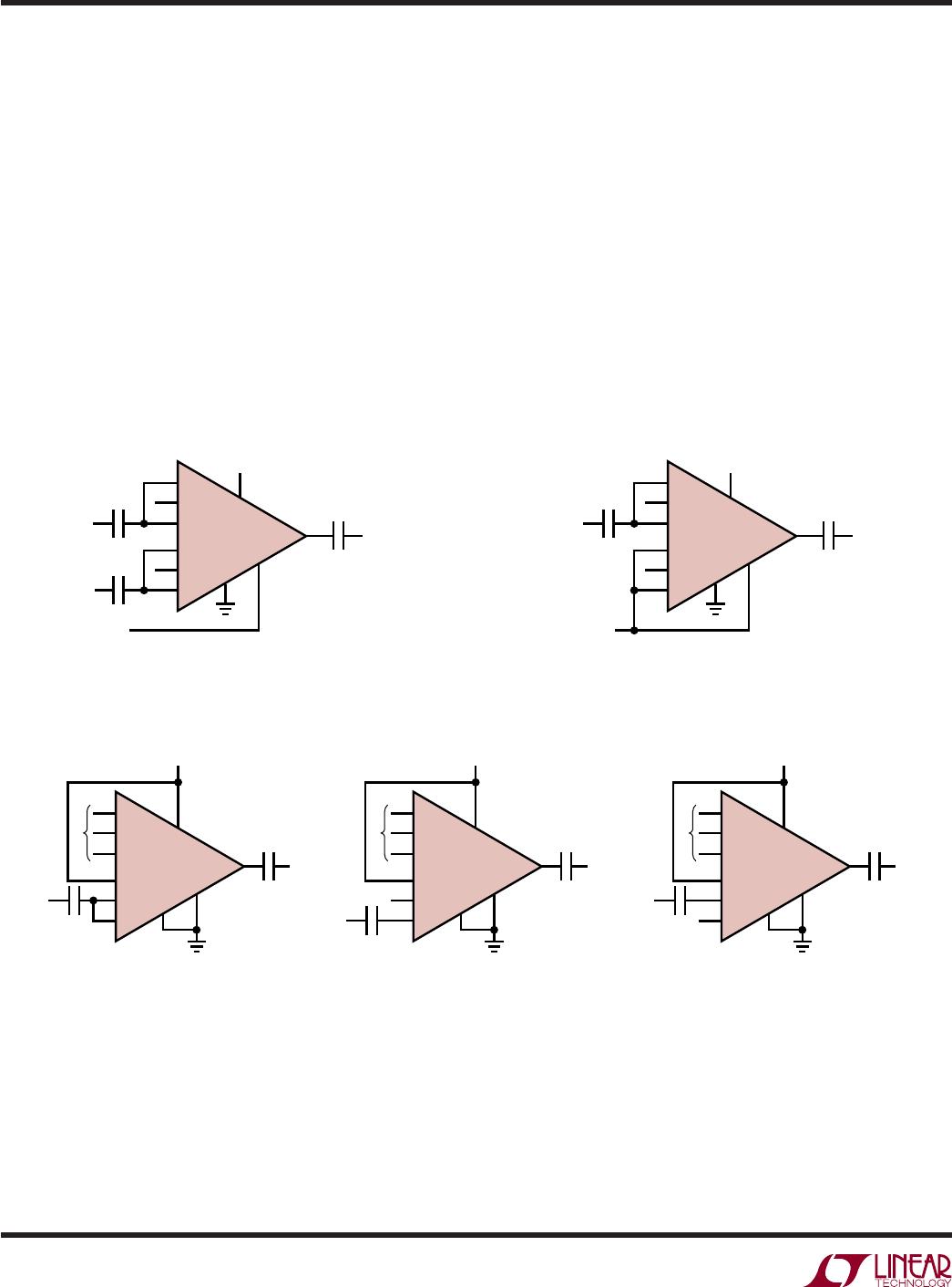
If one of the A parameter configurations in Figure 3 is
preferred, or the use of an external biasing source is
desired, the P and REF input connections shown grounded
in a Figure 3 circuit may be instead driven by a V
BIAS
voltage to establish a quiescent operating point for the
input and output pins. The V
IN
connections of the Figure 3
circuit are then driven via a coupling capacitor. Any
grounded M inputs for the desired G configuration (refer
to Figure 2) must be individually or collectively
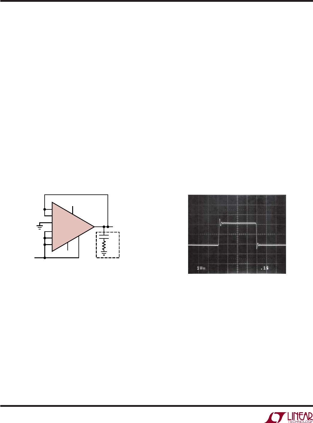
AC-coupled to ground. Figure 8 illustrates a complete
example circuit of an externally biased AC-coupled nonin-
verting amplifier. The V
BIAS
source impedance should be
low (a few ohms) to avoid degrading the inherent accuracy
of the LT1995. 0.013% of additional Gain Error for each
ohm of resistance on the REF pin is typical.
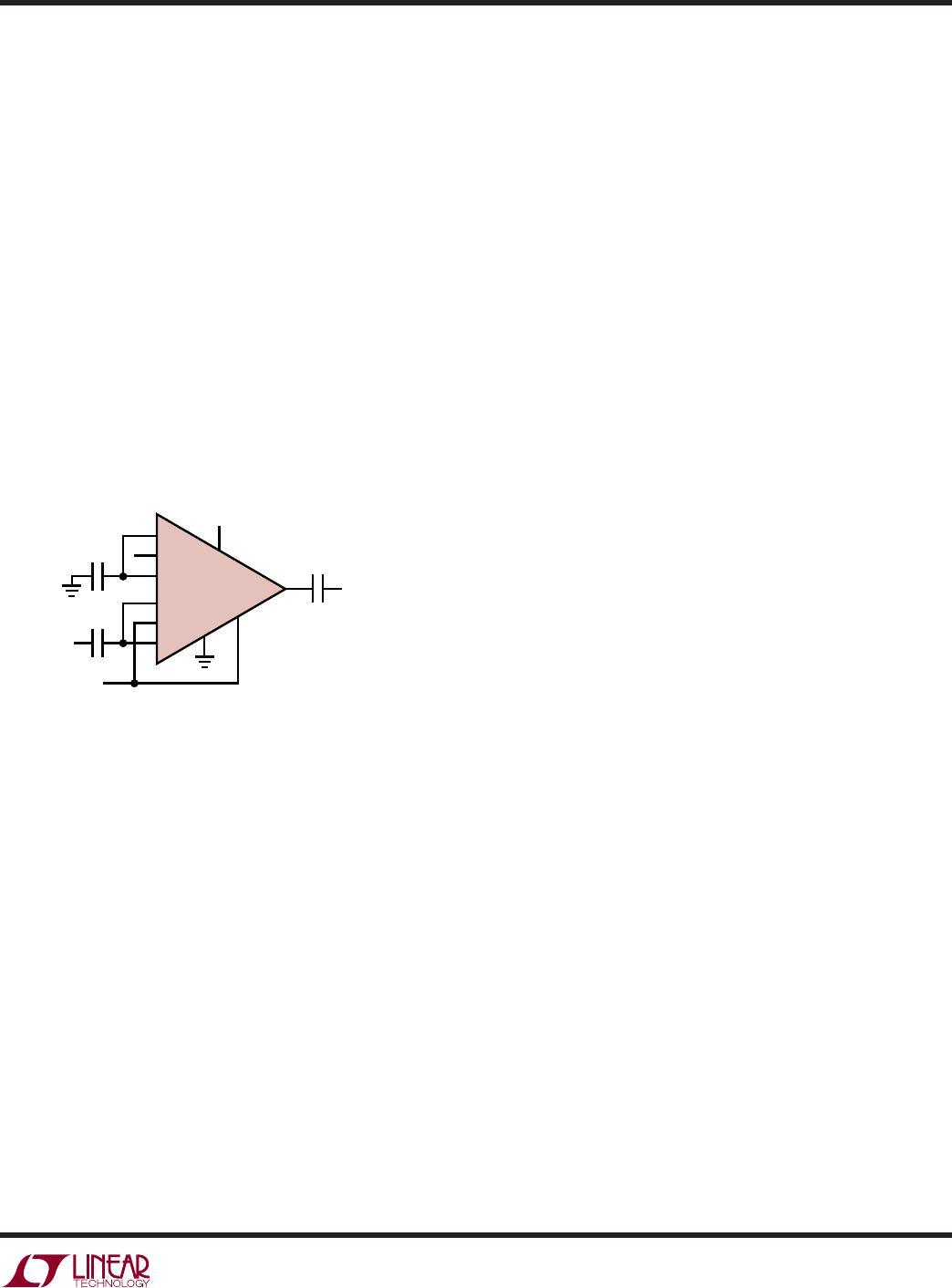
at room temperature, and to within 0.3% over tempera-
ture. The temperature coefficient of the resistors is typi-
cally –30ppm/°C. The resistors have been sized to accom-
modate 15V across each resistor, or in terms of power,
225mW in the 1k resistors, 113mW in the 2k resistors, and
56mW in the 4k resistors.
Power Supply Considerations
As with any high speed amplifier, the LT1995 printed
circuit layout should utilize good power supply decoupling
practices. Good decoupling will typically consist of one or
more capacitors employing the shortest practical inter-
connection traces and direct vias to a ground plane. This
practice minimizes inductance at the supply pins so the
impedance is low at the operating frequencies of the part,
thereby suppressing feedback or crosstalk artifacts that
might otherwise lead to extended settling times, fre-
quency response anomalies, or even oscillation. For high
speed parts like the LT1995, 10nF ceramics are suitable
close-in bypass capacitors, and if high currents are being
delivered to a load, additional 4.7µF capacitors in parallel
can help minimize induced power supply transients.
Because unused input pins are connected via resistors to
the input of the op amp, excessive capacitances on these
pins will degrade the rise time, slew rate, and step re-
sponse of the output. Therefore, these pins should not be
connected to large traces which would add capacitance
when not in use.
Since the LT1995 has a wide operating supply voltage
range, it is possible to place the part in situations of
relatively high power dissipation that may cause excessive
die temperatures to develop. Maximum junction tempera-
ture (T
J
) is calculated from the ambient temperature (T
A
)
M4
M2
M1
P1
P2
P4
8
9
10
1
2
3
V
OUT
CONFIGURATION EXAMPLE:
A = 0.625
G = 6.00
(V
OUT
/V
IN
= 3.75V)
C
OUT
V
BIAS
V
IN
+V
6
4
5
1995 F08
7
LT1995
REF
C
BYP
C
IN
Figure 8. AC-Coupled Noninverting Amplifier
with External Bias Source (Example)
Resistor Considerations
The resistors in the LT1995 are very well matched, low
temperature coefficient thin film based elements. Although
their absolute tolerance is fairly wide (typically ±5% but
±25% worst case), the resistor matching is to within 0.2%
18
LT1995
1995fb
APPLICATIO S I FOR ATIO
WUUU
and power dissipation (P
D
) as follows for a nominal PCB
layout:
T
J
= T
A
+ (P
D
θ
JA
)
For example, in order to maintain a maximum junction
temperature of 150°C at 85°C ambient in an MS10 pack-
age, the power must be limited to 0.4W. It is important to
note that when operating at ±15V supplies, the quiescent
current alone will typically account for 0.24W, so careful
thermal management may be required if high load cur-
rents and high supply voltages are involved. By additional
copper area contact to the supply pins or effective thermal
coupling to extended ground plane(s), the thermal imped-
ance can be reduced to 130°C/W in the MS10 package. A
substantial reduction in thermal impedance of the DD10
package down to about 50°C/W can be achieved by
connecting the Exposed Pad on the bottom of the package
to a large PC board metal area which is either open-
circuited or connected to V
S
.
M4
M2
M1
P1
P2
P4
8
9
10
1
2
3
V
OUT
10nF
47
V
IN
+V
–V
6
4
CONFIGURATION EXAMPLE:
G = 1.14
5
1995 F09
7
LT1995
REF
Figure 9. Optional Frequency Compensation
Network for (1 G 2)
Frequency Compensation
The LT1995 comfortably drives heavy resistive loads such
as back-terminated cables and provides nicely damped
responses for all gain configurations when doing so.
Small capacitances are included in the on-chip resistor
network to optimize bandwidth in the basic difference gain
configurations of Figure 1. For the noninverting configura-
tions of Figure 2, where the gain parameter G is 2 or less,
significant overshoot can occur when driving light loads.
For these low gain cases, providing an RC output network
as shown in Figure 9 to create an artificial load at high
frequency will assure good damping behavior.
Figure 10. Step Response of Circuit in Figure 9

LT1995IDD#TRPBF

Mfr. #:
Manufacturer:
Analog Devices Inc.
Description:
Differential Amplifiers 30MHz, 1000V/ s Gain Sel Amp
Lifecycle:
New from this manufacturer.
Delivery:
DHL FedEx Ups TNT EMS
Payment:
T/T Paypal Visa MoneyGram Western Union