12
LT1995
1995fb
APPLICATIO S I FOR ATIO
WUUU
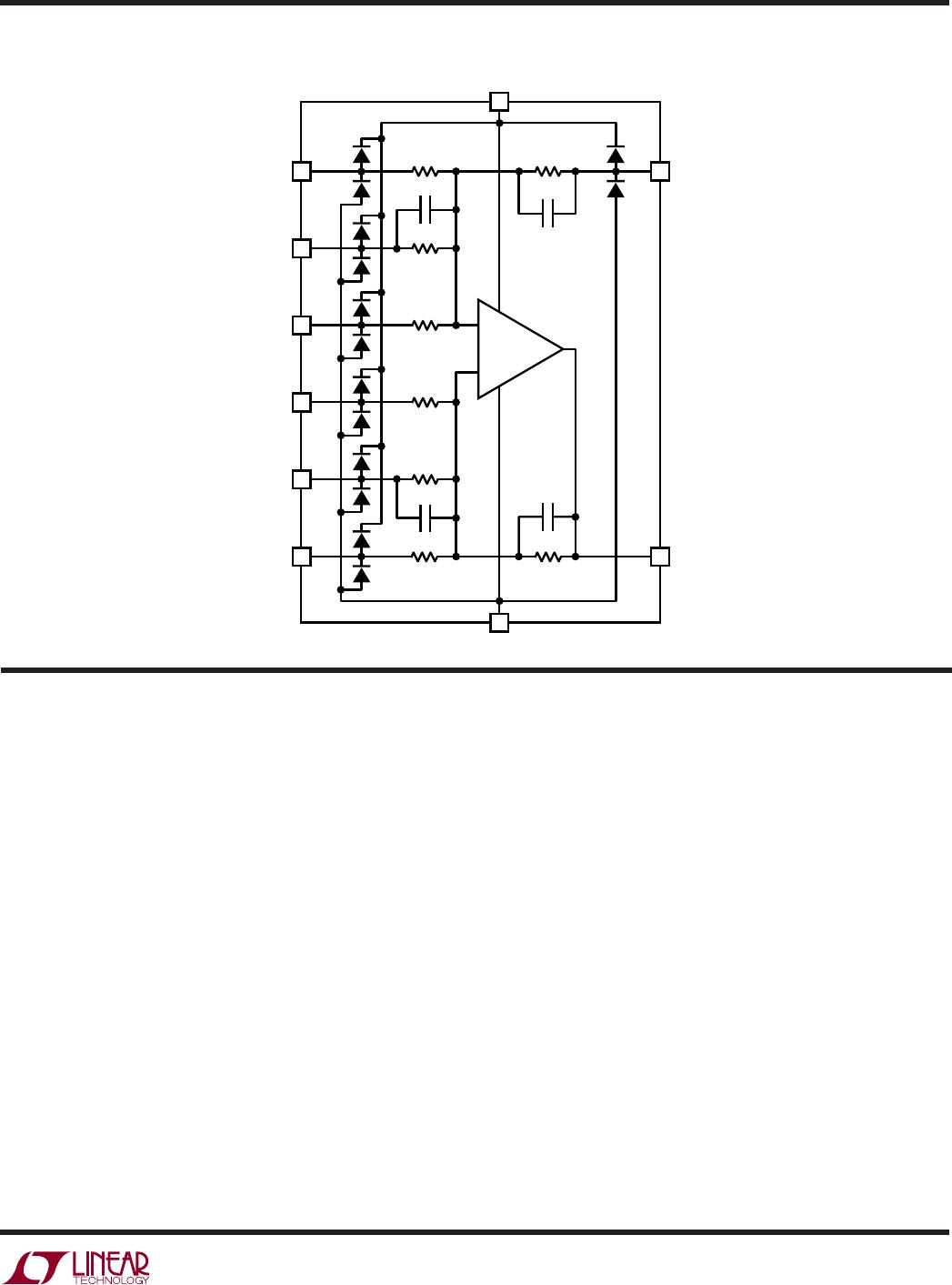
As shown in Figure 1, the options for fixed gain G include:
1, 1.33, 1.67, 2, 3, 4, 5, 6 and 7, all achieved by pin-
strapping alone. With split-supply applications where the
output is to be ground referenced, the V
REF
input is simply
tied to ground. The input common mode voltage is
rejected by the high CMRR of the part within the usable
input range.
Inverting Gain Amplifier
The LT1995 can be connected as an inverting gain ampli-
fier with an output function given by:
V
OUT
= –(G • V
IN
–
) + V
REF
As shown in Figure 1, the options for fixed gain G include:
1, 1.33, 1.67, 2, 3, 4, 5, 6 and 7, all achieved by pin
strapping alone. The V
IN
+
connection used in the differ-
ence amp configuration is simply tied to ground (or a low
impedance potential equal to the input signal bias to create
an input “virtual ground”). With split-supply applications
where the output is to be ground referenced, the V
REF
input
is simply tied to ground as well.
Noninverting Gain Buffer Amplifier
The LT1995 can be connected as a high input impedance
noninverting gain buffer amplifier with an output function
given by:
V
OUT
= G • V
IN
As shown in Figure 2, the options for fixed gain G include:
1, 1.14, 1.2, 1.33, 1.4, 1.6, 2, 2.33, 2.66, 3, 4, 5, 6, 7 and
8, all achieved by pin strapping alone. With single supply
applications, the grounded M input pins may be tied to a
low impedance potential equal to the input signal bias to
create a “virtual ground” for both the input and output
signals. While there is no input attenuation from V
IN
to the
internal noninverting op amp port in these configurations,
the P connections vary to minimize offset by providing
balanced input resistances to the internal op amp.
Noninverting Gain Amplifier Input Attenuation
The LT1995 can also be connected as a noninverting gain
amplifier having an input attenuation network to provide a
wide range of additional noninverting gain options. In
combination with the feedback configurations for gains of
G shown in Figure 2 (connections to the M inputs), the P
and REF inputs may be connected to form several resistor
divider attenuation ratios A, so that a compound output
function is given by:
V
OUT
= A • G • V
IN
As shown in Figure 3, the options for fixed attenuation A
include 0.875, 0.857, 0.833, 0.8, 0.75, 0.714, 0.667, 0.625
and 0.571, all achieved by pin strapping alone. With just
the attenuation configurations of Figure 3 and the feed-
back configurations of Figure 2, seventy-three unique
composite gains in the range of 1 to 8 are available (many
options for gain below unity also exist). Figure 3 does not
include the additional pin-strap configurations offering A
values of 0.5, 0.429, 0.375, 0.333, 0.286, 0.25, 0.2, 0.167,
0.143 and 0.125, as these values tend to compromise the
low noise performance of the part and don’t generally
contribute many more unique gain options. It should be
noted that with these configurations some degree of
imbalance will generally exist between the effective resis-
tances R
P
and R
M
seen by the internal op amp input ports,
noninverting and inverting, respectively. Depending on
the specific combination of A and G, the following DC
offset error due to op amp input bias current (I
B
) should be
anticipated: The I
B
of the internal op amp is typically 0.6µA
and is prepackage tested to a limit of 2µA. Additional
output-referred offset = I
B
• (R
P
– R
M
) • G. In some
configurations, this could be as much as 1.7mV • G
additional output offset. The I
OS
of the internal op amp is
typically 120nA and is prepackage tested to a limit of
350nA. The Electrical Characteristics table includes the
effects of I
B
and I
OS
.