4
LT1995
1995fb
SYMBOL PARAMETER CONDITIONS V
SUPPLY
MIN TYP MAX UNITS
GE Gain Error V
OUT
= ±12V, R
L
= 1k, G = 1 ±15V 0.05 0.25 %
V
OUT
= ±12V, R
L
= 1k, G = 2 ±15V 0.05 0.25 %
V
OUT
= ±12V, R
L
= 1k, G = 4 ±15V 0.05 0.25 %
V
OUT
= ±2.5V, R
L
= 500, G = 1 ±5V 0.05 0.25 %
V
OUT
= ±2.5V, R
L
= 150, G = 1 ±5V 0.05 0.35 %
V
OS
Input Offset Voltage G = 1 (MS10) ±15V 1.1 6.5 mV
Referred to Input (Note 7) G = 1 (DD10) ±15V
1.5 11.5 mV
G = 2 (MS10) ±15V
0.8 5.5 mV
G = 2 (DD10) ±15V
1.2 9 mV
G = 4 (MS10) ±15V
0.7 5 mV
G = 4 (DD10) ±15V
0.9 7.5 mV
G = 1 (MS10) ±5V
1 6.5 mV
G = 1 (DD10) ±5V
1.4 11.5 mV
G = 1 (MS10) ±2.5V
1 6.5 mV
G = 1 (DD10) ±2.5V
1.3 11.5 mV
V
OS
TC Input Offset Voltage Drift G = 1 (MS10) ±15V 10 26 µV/°C
Referred to Input (Note 9) G = 1 (DD10) ±15V
10 35 µV/°C
V
OS_OA
Op Amp Input Offset Voltage G = 1 (MS10) ±2.5V, ±5V, ±15V 0.55 3.25 mV
(Note 10) G = 1 (DD10) ±2.5V, ±5V, ±15V
0.75 5.75 mV
Input Voltage Range G = 1 ±15V ±15 ±15.5 V
±5V
±5 ±5.5 V
±2.5V
±1 ±1.5 V
CMRR Common Mode Rejection Ratio V
CM
= ±15V, G = 1 ±15V 63 77 dB
Referred to Input V
CM
= ±15V, G = 2 ±15V 69 83 dB
V
CM
= ±15V, G = 4 ±15V 73 86 dB
V
CM
= ±5V, G = 1 ±5V 62 72 dB
V
CM
= ±1V, G = 1 ±2.5V 59 66 dB
PSRR Power Supply Rejection Ratio P1 = M1 = 0V, G = 1, V
S
= ±2.5V to ±15V 76 86 dB
V
OUT
Output Voltage Swing R
L
= 1k ±15V ±13.1 ±14 V
R
L
= 500 ±15V ±12.6 ±13.5 V
R
L
= 500 ±5V ±3.4 ±4V
R
L
= 500 ±2.5V ±1.2 ±2V
I
SC
Short-Circuit Current G = 1 ±15V ±55 ±115 mA
SR Slew Rate G = –2, V
OUT
= ±12V, P2 = 0V ±15V 600 900 V/µs
Measured at V
OUT
= ±10V
I
S
Supply Current G = 1 ±15V 7.9 10.5 mA
±5V
7.4 9.9 mA
The denotes the specifications which apply over the 0°C T
A
70°C.
Difference Amplifier Configuration. V
REF
= V
CM
= 0V and unused gain pins are unconnected, unless otherwise noted.
ELECTRICAL CHARACTERISTICS
The denotes the specifications which apply over the –40°C T
A
85°C.
Difference Amplifier Configuration. V
REF
= V
CM
= 0V and unused gain pins are unconnected, unless otherwise noted.
SYMBOL PARAMETER CONDITIONS V
SUPPLY
MIN TYP MAX UNITS
GE Gain Error V
OUT
= ±12V, R
L
= 1k, G = 1 ±15V 0.05 0.3 %
V
OUT
= ±12V, R
L
= 1k, G = 2 ±15V 0.05 0.35 %
V
OUT
= ±12V, R
L
= 1k, G = 4 ±15V 0.05 0.35 %
V
OUT
= ±2.5V, R
L
= 500, G = 1 ±5V 0.05 0.3 %
V
OUT
= ±2.5V R
L
= 150, G = 1 ±5V 0.05 0.5 %
5
LT1995
1995fb
SYMBOL PARAMETER CONDITIONS V
SUPPLY
MIN TYP MAX UNITS
V
OS
Input Offset Voltage G = 1 (MS10) ±15V 1.2 7.5 mV
Referred to Input (Note 7) G = 1 (DD10) ±15V
1.6 13 mV
G = 2 (MS10) ±15V
0.9 6 mV
G = 2 (DD10) ±15V
1.2 10 mV
G = 4 (MS10) ±15V
0.7 5.5 mV
G = 4 (DD10) ±15V
0.9 8.5 mV
G = 1 (MS10) ±5V
1.1 7.5 mV
G = 1 (DD10) ±5V
1.4 13 mV
G = 1 (MS10) ±2.5V
1.1 7.5 mV
G = 1 (DD10) ±2.5V
1.5 13 mV
V
OS
TC Input Offset Voltage Drift G = 1 (MS10) ±15V 10 26 µV/°C
Referred to Input (Note 9) G = 1 (DD10) ±15V
10 35 µV/°C
V
OS_OA
Op Amp Input Offset Voltage G = 1 (MS10) ±2.5V, ±5V, ±15V 0.6 3.75 mV
(Note 10) G = 1 (DD10) ±2.5V, ±5V, ±15V
0.8 6.5 mV
Input Voltage Range G = 1 ±15V ±15 ±15.5 V
±5V
±5 ±5.5 V
±2.5V
±1 ±1.5 V
CMRR Common Mode Rejection Ratio V
CM
= ±15V, G = 1 ±15V 62 77 dB
Referred to Input V
CM
= ±15V, G = 2 ±15V 68 83 dB
V
CM
= ±15V, G = 4 ±15V 72 86 dB
V
CM
= ±5V, G = 1 ±5V 61 72 dB
V
CM
= ±1V, G = 1 ±2.5V 57 66 dB
PSRR Power Supply Rejection Ratio P1 = M1 = 0V, G = 1, V
S
= ±2.5V to ±15V 74 86 dB
V
OUT
Output Voltage Swing R
L
= 1k ±15V ±13 ±14 V
R
L
= 500 ±15V ±12.5 ±13.5 V
R
L
= 500 ±5V ±3.3 ±4V
R
L
= 500 ±2.5V ±1.1 ±2V
I
SC
Short-Circuit Current G = 1 ±15V ±50 ±105 mA
SR Slew Rate G = –2, V
OUT
= ±12V, P2 = 0V ±15V 550 900 V/µs
Measured at V
OUT
= ±10V
I
S
Supply Current G = 1 ±15V 8.0 11.0 mA
±5V
7.6 10.4 mA
The denotes the specifications which apply over the –40°C T
A
85°C.
Difference Amplifier Configuration. V
REF
= V
CM
= 0V and unused gain pins are unconnected, unless otherwise noted.
ELECTRICAL CHARACTERISTICS
Note 1: Absolute Maximum Ratings are those values beyond which the life
of a device may be impaired.
Note 2: The inputs are protected by diodes connected to V
S
+
and V
S
.
If an input goes beyond the supply range, the input current should be
limited to 10mA.
Note 3: A heat sink may be required to keep the junction temperature
below absolute maximum.
Note 4: The LT1995C and LT1995I are guaranteed functional over the
operating temperature range of –40°C to 85°C.
Note 5: The LT1995C is guaranteed to meet specified performance from
0°C to 70°C. The LT1995C is designed, characterized and expected to
meet specified performance from –40°C to 85°C but is not tested or QA
sampled at these temperatures. The LT1995I is guaranteed to meet
specified performance from –40°C to 85°C.
Note 6: Thermal resistance (θ
JA
) varies with the amount of PC board metal
connected to the leads. The specified values are for short traces connected
to the leads. If desired, the thermal resistance can be reduced slightly in
the MS package to about 130°C/W by connecting the used leads to a
larger metal area. A substantial reduction in thermal resistance down to
about 50°C/W can be achieved by connecting the Exposed Pad on the
bottom of the DD package to a large PC board metal area which is either
open-circuited or connected to V
S
.
Note 7: Input offset voltage is pulse tested and is exclusive of warm-up
drift. V
OS
and V
OS
TC refer to the input offset of the difference amplifier
configuration. The equivalent input offset of the internal op amp can be
calculated from V
OS_OA
= V
OS
• G/(G +1).
Note 8: Full Power bandwidth is calculated from the slew rate measure-
ment: FPBW = SR/2πV
P
.
Note 9: This parameter is not 100% tested.
Note 10: The input offset of the internal op amp is calculated from the
input offset voltage: V
OS_OA
= V
OS
• G/(G +1).
6
LT1995
1995fb
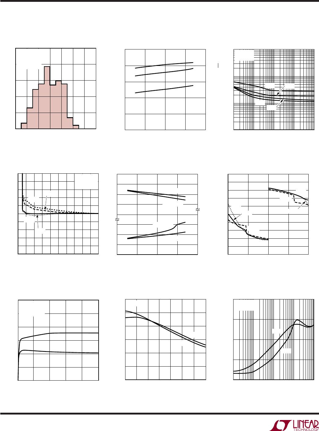
FREQUENCY (Hz)
1
OUTPUT IMPEDACNE ()
10
100
1000
10k 1M 10M 100M
1995 G09
0.1
100k
V
S
= ±15V
T
A
= 25°C
G = 7
G = 1
TEMPERATURE (°C)
–50
OUTPUT SHORT-CIRCUIT CURRENT (mA)
80
100
120
25 75
1995 G08
60
40
–25 0
50 100 125
20
0
V
S
= ±5V
SOURCE
SINK
TIME AFTER POWER ON (MINUTES)
0
0
CHANGE IN INPUT OFFSET VOLTAGE (µV)
50
100
150
200
250
300
1234
1995 G07
5
G = 1
G = 7
V
S
= ±15V
T
A
= 25°C
MS PACKAGE
OUTPUT CURRENT (mA)
–50
OUTPUT VOLTAGE (V)
1995 G06
5025–25 0
V
0.5
1.0
1.5
2.0
3.0
2.5
–1.5
–2.0
–1.0
V
+
–0.5
V
S
= ±5V
25°C
–40°C
85°C
–40°C
85°C
25°C
SUPPLY VOLTAGE (±V)
0
OUTPUT VOLTAGE (V)
1995 G05
20
5
10
15
V
0.5
1.0
1.5
–1.5
–1.0
V
+
–0.5
T
A
= 25°C
R
L
= 500
R
L
= 1k
R
L
= 500
R
L
= 1k
RESISTIVE LOAD (k)
0
CHANGE IN GAIN ERROR (%)
0.05
0.04
0.03
0.01
0.02
0
–0.01
–0.02
–0.03
–0.04
–0.05
8
1995 G04
213579
4
6
10
G = 7
G = 2
V
S
= ±15V
T
A
= 25°C
V
OUT
= ±12V
G = 4
G = 1
FREQUENCY (kHz)
10
INPUT VOLTAGE NOISE (nV/Hz)
100
0.01 1 10 100
1995 G03
1
0.1
1000
V
S
= ±15V
T
A
= 25°C
G = 1
G = 7
G = 2
G = 4
SUPPLY VOLTAGE (±V)
0
SUPPLY CURRENT (mA)
4
6
20
1995 G02
2
0
5
10
15
10
8
T
A
= 125°C
T
A
= 25°C
T
A
= –55°C
INPUT OFFSET VOLTAGE (mV)
–3.5
0
NUMBER OF UNITS (%)
10
25
–1.5
0.5
1.5
1995 G01
5
20
15
–2.5
–0.5
2.5
3.5
V
S
= ±15V
V
CM
= 0V
G = 1
MS PACKAGE
TYPICAL PERFOR A CE CHARACTERISTICS
UW
Supply Current vs Supply Voltage
and Temperature Input Noise Spectral Density
Change in Gain Error
vs Resistive Load
Output Voltage Swing vs Supply
Voltage
Output Voltage Swing vs Load
Current
(Difference Amplifier Configuration)
Warm-Up Drift vs Time
Output Short-Circuit Current
vs Temperature Output Impedance vs Frequency
V
OS
Distribution

LT1995IDD#TRPBF

Mfr. #:
Manufacturer:
Analog Devices Inc.
Description:
Differential Amplifiers 30MHz, 1000V/ s Gain Sel Amp
Lifecycle:
New from this manufacturer.
Delivery:
DHL FedEx Ups TNT EMS
Payment:
T/T Paypal Visa MoneyGram Western Union