10
FN8191.4
January 15, 2009
Write Wiper Counter Register (WCR) to Data Register (DR)
Increment/Decrement Wiper Counter Register (WCR)
Global XFR Data Register (DR) to Wiper Counter Register (WCR)
Global XFR Wiper Counter Register (WCR) to Data Register (DR)
Symbol Table
Guidelines for Calculating Typical Values of Bus
Pull-Up Resistors
S
T
A
R
T
DEVICE TYPE
IDENTIFIER
DEVICE
ADDRESSES S
A
C
K
INSTRUCTION
OPCODE
DR AND WCR
ADDRESSES S
A
C
K
S
T
O
P
HIGH-VOLTAGE
WRITE CYCLE
0 1 0 1 A3 A2 A1 A0 1 1 1 0 R1 R0 P1 P0
S
T
A
R
T
DEVICE TYPE
IDENTIFIER
DEVICE
ADDRESSES S
A
C
K
INSTRUCTION
OPCODE
WCR
ADDRESSES S
A
C
K
INCREMENT/DECREMENT
(SENT BY MASTER ON SDA) S
T
O
P
0101A3A2A1A0 0 01 000P1P0 I/DI/D. . . .I/DI/D
S
T
A
R
T
DEVICE TYPE
IDENTIFIER
DEVICE
ADDRESSES S
A
C
K
INSTRUCTION
OPCODE
DR
ADDRESSES S
A
C
K
S
T
O
P
0 1 0 1 A3A2A1A0 0 0 0 1 R1R0 0 0
S
T
A
R
T
DEVICE TYPE
IDENTIFIER
DEVICE
ADDRESSES S
A
C
K
INSTRUCTION
OPCODE
DR
ADDRESSES S
A
C
K
S
T
O
P
HIGH-VOLTAGE
WRITE CYCLE
0 1 0 1 A3A2A1A0 1 0 0 0 R1R0 0 0
WAVEFORM INPUTS OUTPUTS
MUST BE
STEADY
WILL BE
STEADY
MAY CHANGE
FROM LO W TO
HIGH
WILL CHANGE
FROM LOW TO
HIGH
MAY CHANGE
FROM HIGH TO
LOW
WILL CHANGE
FROM HIGH TO
LOW
DON’T CARE:
CHANGES
ALLOWED
CHANGING:
STATE NOT
KNOWN
N/A CENTER LINE
IS HIGH
IMPEDANCE
120
100
80
40
60
20
20 40 60 80 100 120
0
0
RESISTANCE (Κ)
BUS CAPACITANCE (pF)
Min.
Resistance
MAX.
RESISTANCE
R
MAX
=
C
BUS
t
R
R
MIN
=
I
OL MIN
V
CC MAX
=1.8kΩ
X9408
11
FN8191.4
January 15, 2009
Absolute Maximum Ratings Thermal Information
Supply Voltage (V
CC
Limits)
X9408. . . . . . . . . . . . . . . . . . . . . . . . . . . . . . . . . . . . . . . 5V ±10%
X9408-2.7. . . . . . . . . . . . . . . . . . . . . . . . . . . . . . . . . . 2.7V to 5.5V
Voltage on SDA, SCL any address input
with respect to V
SS
: . . . . . . . . . . . . . . . . . . . . . . . . . . . -1V to +7V
Voltage on V+ (Referenced to V
SS
). . . . . . . . . . . . . . . . . . . . . . .10V
Voltage on V- (Referenced to V
SS
) . . . . . . . . . . . . . . . . . . . . . . -10V
(V+) - (V-). . . . . . . . . . . . . . . . . . . . . . . . . . . . . . . . . . . . . . . . . . .12V
I
W
(10s) . . . . . . . . . . . . . . . . . . . . . . . . . . . . . . . . . . . . . . . . . . ±6mA
Any VH/RH, VL/RL, VW/RW . . . . . . . . . . . . . . . . . . . . . . . . V- to V+
Temperature Under Bias . . . . . . . . . . . . . . . . . . . . .-65°C to +135°C
Storage Temperature. . . . . . . . . . . . . . . . . . . . . . . .-65°C to +150°C
Pb-Free Reflow Profile. . . . . . . . . . . . . . . . . . . . . . . . .see link below
http://www.intersil.com/pbfree/Pb-FreeReflow.asp
Operating Conditions
Temperature Range
Commercial . . . . . . . . . . . . . . . . . . . . . . . . . . . . . . . 0°C to +70°C
Industrial. . . . . . . . . . . . . . . . . . . . . . . . . . . . . . . . .-40°C to +85°C
CAUTION: Do not operate at or near the maximum ratings listed for extended periods of time. Exposure to such conditions may adversely impact product reliability and
result in failures not covered by warranty.
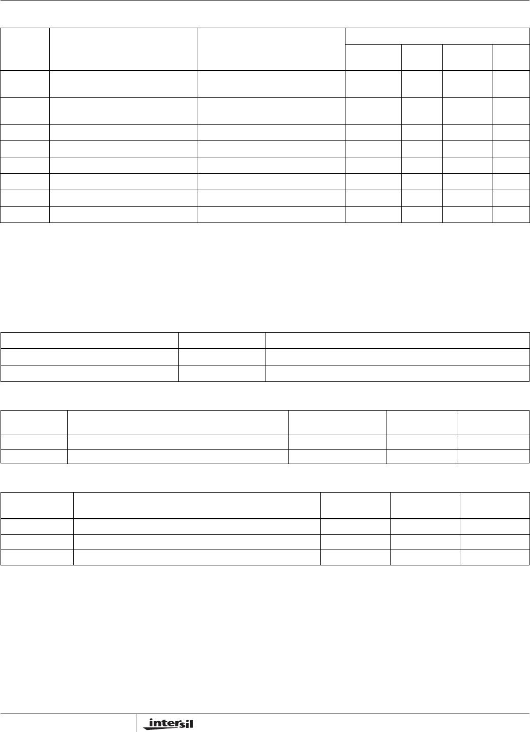
Analog Specifications (Over recommended operating conditions unless otherwise stated.)
SYMBOL PARAMETER TEST CONDITION
LIMITS
MIN
(Note 6)
TYP
(Note 4)
MAX
(Note 6) UNIT
R
TOTAL
End to end resistance tolerance -20 +20 %
Power rating +25°C, each pot 50 mW
R
W
Wiper resistance I
W
= (V
H
- V
L
)/R
TOTAL
@ V+, V- = ±3V
150 250 Ω
I
W
= (V
H
- V
L
)/R
TOTAL
@ V+, V- = ±5V
40 100 Ω
V
V
+ Voltage on V+ pin X9408 +4.5 +5.5 V
X9408-2.7 +2.7 +5.5
V
V
- Voltage on V- pin X9408 -5.5 -4.5 V
X9408-2.7 -5.5 -2.7
V
TERM
Voltage on any V
H
/R
H
, V
L
/R
L
or
V
W
/R
W
pin
V- V+ V
Noise Ref: 1kHz -120 dBV
Resolution (Note 4) 1.6 %
Absolute linearity (Note 1) V(V
wn
/R
wn
)
(actual)
-
V(V
wn
/R
wn
)
(expected)
(Note 4)
-1 +1 MI
(Note 3)
Relative linearity (Note 2) V(V
w(n+1)
/R
w(n+1)
) -
[V(V
w(n)
/R
w(n)
) + MI] (Note 4)
-0.2 +0.2 MI
(Note 3)
Temperature coefficient of R
TOTAL
(Note 4) ±300 ppm/°C
Ratiometric Temperature Coefficient (Note 4) ±20 ppm/°C
C
H
/C
L
/C
W
Potentiometer Capacitances See Macro model 10/10/25 pF
I
AL
V
H
/R
H
, V
L
/R
L
, V
W
/R
W
Leakage
Current
V
IN
= V- to V+. Device is in Stand-
by mode.
0.1 10 µA
X9408
12
FN8191.4
January 15, 2009
NOTES:
1. Absolute linearity is utilized to determine actual wiper voltage versus expected voltage as determined by wiper position when used as a
potentiometer.
2. Relative linearity is utilized to determine the actual change in voltage between two successive tap positions when used as a potentiometer. It is
a measure of the error in step size.
3. MI = RTOT/63 or [V(V
H
/R
H
) - V(V
L
/R
L
)]/63, single pot
ENDURANCE AND DATA RETENTION
CAPACITANCE
POWER-UP TIMING
NOTES:
4. Limits should be considered typical and are not production tested.
5. t
PUR
and t
PUW
are the delays required from the time the third (last) power supply (V
CC
, V+ or V-) is stable until the specific
instruction can be issued
6. Parameters with MIN and/or MAX limits are 100% tested at +25°C, unless otherwise specified. Temperature limits established by characterization
and are not production tested.
DC Electrical Specifications (Over recommended operating conditions unless otherwise stated.)
SYMBOL PARAMETER TEST CONDITIONS
LIMITS
MIN
(Note 6)
TYP
(Note 4)
MAX
(Note 6) UNIT
I
CC1
V
CC
supply current (nonvolatile write) f
SCL
= 400kHz, SDA = Open,
Other Inputs = V
SS
5mA
I
CC2
V
CC
supply current (move wiper, write,
read)
f
SCL
= 400kHz, SDA = Open,
Other Inputs = V
SS
250 µA
I
SB
V
CC
current (standby) SCL = SDA = V
CC
, Addr. = V
SS
A
I
LI
Input leakage current 10 µA
I
LO
Output leakage current 10 µA
V
IH
Input HIGH voltage V
CC
x 0.7 V
CC
+0.5 V
V
IL
Input LOW voltage –0.5 V
CC
x 0.1 V
V
OL
Output LOW voltage I
OL
= 3mA 0.4 V
PARAMETER MIN UNIT
Minimum endurance 100,000 Data changes per bit per register
Data retention 100 years
SYMBOL TEST TEST CONDITION
TYP
(Note 4) UNIT
C
I/O
(Note 4) Input/output capacitance (SDA) V
I/O
= 0V 8 pF
C
IN
(Note 4) Input capacitance (A0, A1, A2, A3, and SCL) V
IN
= 0V 6 pF
SYMBOL PARAMETER
MIN
(Note 6)
MAX
(Note 6) UNIT
t
PUR
(Note 5) Power-up to initiation of read operation 1 ms
t
PUW
(Note 5) Power-up to initiation of write operation 5 ms
t
R
V
CC
(Note 6) V
CC
Power-up Ramp 0.2 50 V/msec
X9408

X9408WV24Z-2.7

Mfr. #:
Manufacturer:
Renesas / Intersil
Description:
Digital Potentiometer ICs DL CMOS EEPOT 10KOHM S
Lifecycle:
New from this manufacturer.
Delivery:
DHL FedEx Ups TNT EMS
Payment:
T/T Paypal Visa MoneyGram Western Union