7
FN8191.4
January 15, 2009
SCL
SDA
V
W
/R
W
INC/DEC
CMD
ISSUED
VOLTAGE OUT
t
WRID
FIGURE 6. INCREMENT/DECREMENT TIMING LIMITS
SCL FROM
DATA OUTPUT
1
89
START
ACKNOWLEDGE
MASTER
FROM TRANSMITTER
DATA OUTPUT
FROM RECEIVER
FIGURE 7. ACKNOWLEDGE RESPNSE FROM RECEIVER
X9408
8
FN8191.4
January 15, 2009
Detailed Operation
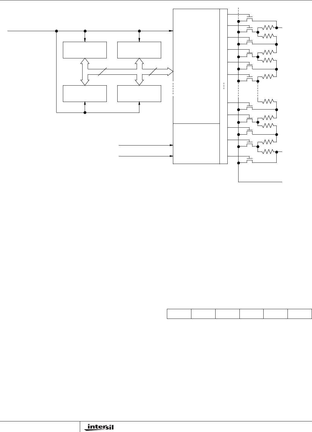
All XDCP potentiometers share the serial interface and
share a common architecture. Each potentiometer has a
Wiper Counter Register and four Data Registers. A detailed
discussion of the register organization and array operation
follows.
Wiper Counter Register
The X9408 contains four Wiper Counter Registers, one for
each XDCP potentiometer. The Wiper Counter Register can
be envisioned as a 6-bit parallel and serial load counter with
its outputs decoded to select one of sixty-four switches along
its resistor array. The contents of the WCR can be altered in
four ways: it may be written directly by the host via the Write
Wiper Counter Register instruction (serial load); it may be
written indirectly by transferring the contents of one of four
associated data registers via the XFR Data Register
instruction (parallel load); it can be modified one step at a
time by the Increment/ Decrement instruction. Finally, it is
loaded with the contents of its data register zero (DR0) upon
power-up.
The WCR is a volatile register; that is, its contents are lost
when the X9408 is powered-down. Although the register is
automatically loaded with the value in R0 upon power-up, it
should be noted this may be different from the value present
at power-down.
Data Registers
Each potentiometer has four nonvolatile Data Registers.
These can be read or written directly by the host and data
can be transferred between any of the four Data Registers
and the WCR. It should be noted all operations changing
data in one of these registers is a nonvolatile operation and
will take a maximum of 10ms.
If the application does not require storage of multiple
settings for the potentiometer, these registers can be used
as regular memory locations that could possibly store
system parameters or user preference data.
Register Descriptions
Four 6-bit Data Registers for each XDCP. (sixteen 6-bit
registers in total). {D5~D0}: These bits are for general
purpose not volatile data storage or for storage of up to four
different wiper values. The contents of Data Register 0 are
automatically moved to the wiper counter register on
power-up.
SERIAL DATA PATH
FROM INTERFACE
CIRCUITRY
REGISTER 0 REGISTER 1
REGISTER 2 REGISTER 3
SERIAL
BUS
INPUT
PARALLEL
BUS
INPUT
WIPER
COUNTER
REGISTER
INC/DEC
LOGIC
UP/DN
CLK
MODIFIED SCL
UP/DN
V
H
/R
H
V
L
/R
L
V
W
/R
W
IF WCR = 00[H] THEN V
W
/R
W
= V
L
/R
L
IF WCR = 3F[H] THEN V
W
/R
W
= V
H
/R
H
8 6
C
O
U
N
T
E
R
D
E
C
O
D
E
(WCR)
FIGURE 8. DETAILED POTENTIOMETER BLOCK DIAGRAM
TABLE 2. DATE REGISTERS, (6-BIT), NONVOLATILE
D5 D4 D3 D2 D1 D0
NV NV NV NV NV NV
(MSB) (LSB)
X9408
9
FN8191.4
January 15, 2009
One 6-bit Wiper Counter Register for each XDCP. (Four 6-bit
registers in total.)
{D5~D0}: These bits specify the wiper position of the
respective XDCP. The Wiper Counter Register is loaded on
power-up by the value in Data Register 0. The contents of
the WCR can be loaded from any of the other Data Register
or directly. The contents of the WCR can be saved in a DR.
Instruction Format
NOTES:
1. “MACK”/”SACK”: stands for the acknowledge sent by the master/slave.
2. “A3 ~ A0”: stands for the device addresses sent by the master.
3. “X”: indicates that it is a “0” for testing purpose but physically it is a “don’t care” condition.
4. “I”: stands for the increment operation, SDA held high during
active SCL phase (high).
5. “D”: stands for the decrement operation, SDA held low during active SCL phase (high).
Read Wiper Counter Register (WCR)
Write Wiper Counter Register (WCR)
Read Data Register (DR)
Write Data Register (DR)
XFR Data Register (DR) to Wiper Counter Register (WCR)
TABLE 3. WIPER COUNTER REGISTER, (6-BIT), VOLATILE
WP5 WP4 WP3 WP2 WP1 WP0
VVVVVV
(MSB) (LSB)
S
T
A
R
T
DEVICE TYPE
IDENTIFIER
DEVICE
ADDRESSES S
A
C
K
INSTRUCTION
OPCODE
WCR
ADDRESSES S
A
C
K
WIPER POSITION
(SENT BY SLAVE ON SDA) M
A
C
K
S
T
O
P
0 1 0 1 A3 A2 A1 A0 1 0 0 1 0 0 P1 P0 0 0 WP
5
WP
4
WP
3
WP
2
WP
1
WP
0
S
T
A
R
T
DEVICE TYPE
IDENTIFIER
DEVICE
ADDRESSES S
A
C
K
INSTRUCTION
OPCODE
WCR
ADDRESSES S
A
C
K
WIPER POSITION
(SENT BY MASTER ON SDA) S
A
C
K
S
T
O
P
0101A3A2A1A0 101000P1P0 00W
P5
W
P4
W
P3
W
P2
W
P1
W
P0
S
T
A
R
T
DEVICE TYPE
IDENTIFIER
DEVICE
ADDRESSES S
A
C
K
INSTRUCTION
OPCODE
DR AND WCR
ADDRESSES S
A
C
K
WIPER POSITION/DATA
(SENT BY SLAVE ON SDA) M
A
C
K
S
T
O
P
0101A3A2A1A0 1011R1R0P1P0 00W
P5
W
P4
W
P3
W
P2
W
P1
W
P0
S
T
A
R
T
DEVICE TYPE
IDENTIFIER
DEVICE
ADDRESSES S
A
C
K
INSTRUCTION
OPCODE
DR AND WCR
ADDRESSES S
A
C
K
WIPER POSITION/DATA
(SENT BY MASTER ON SDA) S
A
C
K
S
T
O
P
HIGH-VOLTAGE
WRITE CYCLE
0101A3A2A1A0 1100R1R0P1P0 00W
P5
W
P4
W
P3
W
P2
W
P1
W
P0
S
T
A
R
T
DEVICE TYPE
IDENTIFIER
DEVICE
ADDRESSES S
A
C
K
INSTRUCTION
OPCODE
DR AND WCR
ADDRESSES S
A
C
K
S
T
O
P
0101A3A2A1A0 1 1 0 1 R1R0P1P0
X9408

X9408WV24Z-2.7

Mfr. #:
Manufacturer:
Renesas / Intersil
Description:
Digital Potentiometer ICs DL CMOS EEPOT 10KOHM S
Lifecycle:
New from this manufacturer.
Delivery:
DHL FedEx Ups TNT EMS
Payment:
T/T Paypal Visa MoneyGram Western Union