13
FN8191.4
January 15, 2009
Power-up Requirements
(Power-up sequencing can affect correct recall of the wiper
registers).
The preferred power-on sequence is as follows: First V-,
then V
CC
and V+, and then the potentiometer pins, V
H
/R
H
,
V
L
/R
L
, and V
W
/R
W
. Voltage should not be applied to the
potentiometer pins before V+ or V- is applied. The V
CC
ramp
rate specification should be met, and any glitches or slope
changes in the V
CC
line should be held to <100mV if
possible. If V
CC
powers down, it should be held below 0.1V
for more than 1 second before powering up again in order for
proper wiper register recall. Also, V
CC
should not reverse
polarity by more than 0.5V. Recall of wiper position will not
be complete until V
CC
, V+ and V- reach their final value.
A.C. Test Conditions
Equivalent A.C. Load Circuit
Circuit #3 SPICE Macro Model
I
nput pulse levels V
CC
x 0.1 to V
CC
x 0.9
Input rise and fall times 10ns
Input and output timing level V
CC
x 0.5
5V
1533Ω
100PF
SDA OUTPUT
10pF
V
H
/R
H
R
TOTAL
C
H
25pF
C
W
C
L
10pF
V
W
/R
W
V
L
/R
L
X9408
14
FN8191.4
January 15, 2009
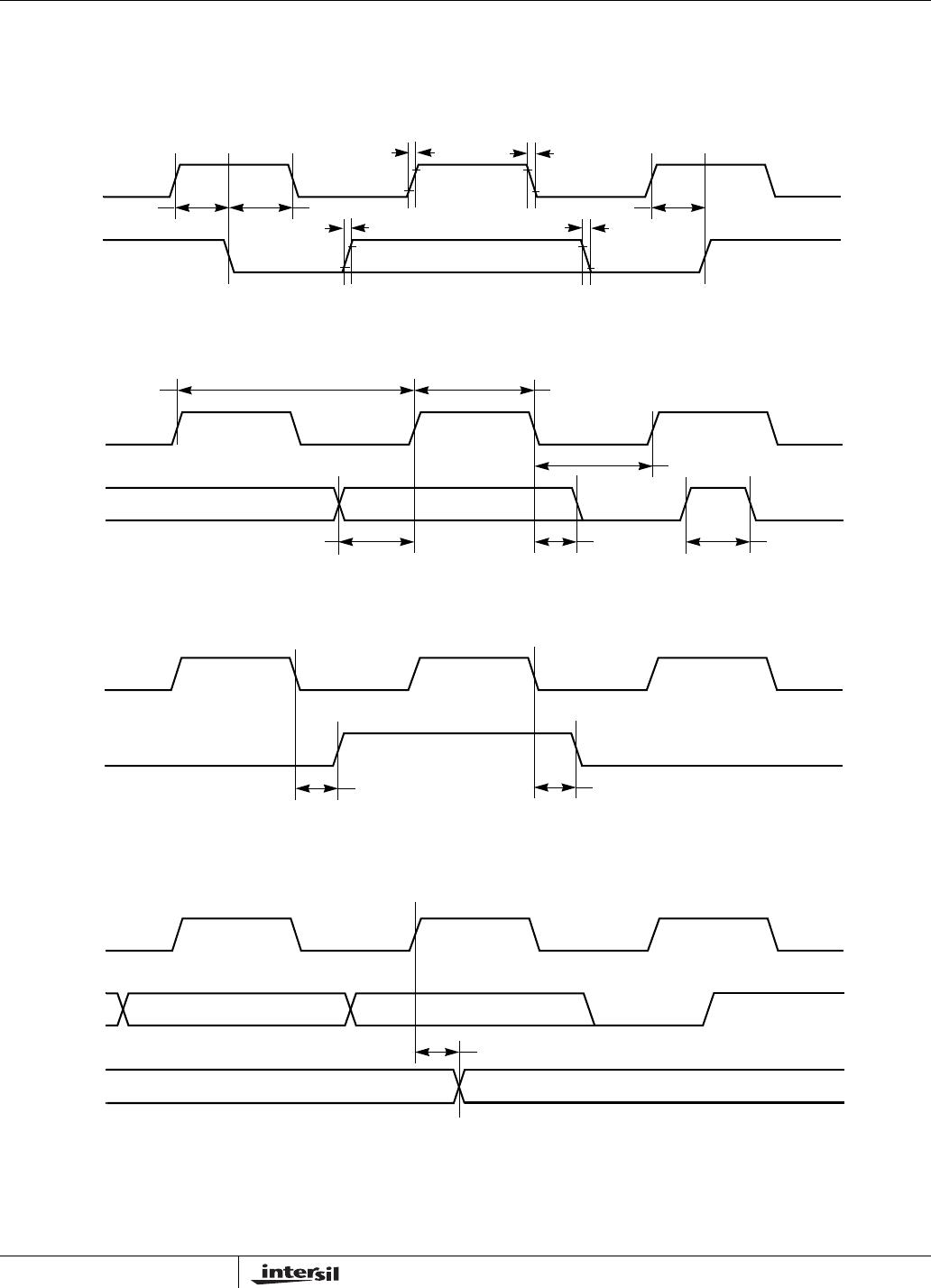
AC Timing (Over recommended operating condition)
HIGH-VOLTAGE WRITE CYCLE TIMING
XDCP TIMING
SYMBOL PARAMETER
MIN
(Note 5)
MAX
(Note 5) UNIT
f
SCL
Clock frequency 400 kHz
t
CYC
Clock cycle time 2500 ns
t
HIGH
Clock high time 600 ns
t
LOW
Clock low time 1300 ns
t
SU:STA
Start setup time 600 ns
t
HD:STA
Start hold time 600 ns
t
SU:STO
Stop setup time 600 ns
t
SU:DAT
SDA data input setup time 100 ns
t
HD:DAT
SDA data input hold time 30 ns
t
R (Note 7)
SCL and SDA rise time 300 ns
t
F (Note 7)
SCL and SDA fall time 300 ns
t
AA
SCL low to SDA data output valid time 900 ns
t
DH
SDA Data output hold time 50 ns
T
I
Noise suppression time constant at SCL and SDA inputs 50 ns
t
BUF
Bus free time (prior to any transmission) 1300 ns
t
SU:WPA
WP, A0, A1, A2 and A3 setup time 0 ns
t
HD:WPA
WP, A0, A1, A2 and A3 hold time
0ns
NOTES:
7. This parameter is not production tested. Parameter established by characterization.
SYMBOL PARAMETER
TYP.
(Note 4)
MAX.
(Note 6) UNIT
t
WR
High-voltage write cycle time (store instructions) 5 10 ms
SYMBOL PARAMETER
MIN.
(Note 5)
MAX.
(Note 6) UNIT
t
WRPO
Wiper response time after the third (last) power supply is stable 10 µs
t
WRL
Wiper response time after instruction issued (all load instructions) 10 µs
t
WRID
Wiper response time from an active SCL/SCK edge (increment/decrement instruction) 10 µs
X9408
15
FN8191.4
January 15, 2009
Timing Diagrams
Start and Stop Timing
g
Input Timing
Output Timing
XDCP Timing (for All Load Instructions)
t
SU:STA
t
HD:STA
t
SU:STO
SCL
SDA
t
R
(START) (STOP)
t
F
t
R
t
F
SCL
SDA
t
HIGH
t
LOW
t
CYC
t
HD:DAT
t
SU:DAT
t
BUF
SCL
SDA
t
DH
t
AA
SCL
SDA
VWx
(STOP)
LSB
t
WRL
X9408

X9408WV24Z-2.7

Mfr. #:
Manufacturer:
Renesas / Intersil
Description:
Digital Potentiometer ICs DL CMOS EEPOT 10KOHM S
Lifecycle:
New from this manufacturer.
Delivery:
DHL FedEx Ups TNT EMS
Payment:
T/T Paypal Visa MoneyGram Western Union