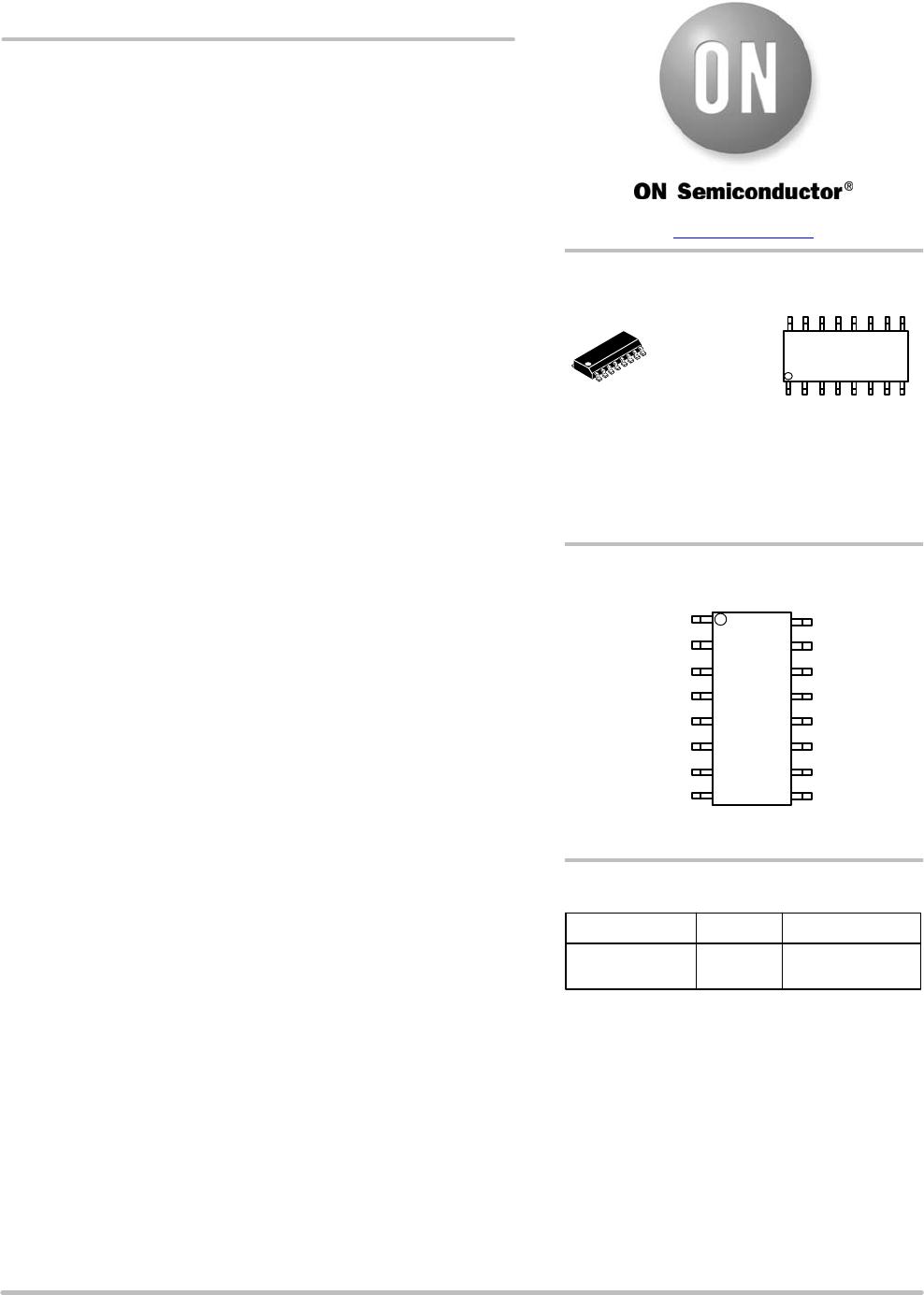
NCL30051
www.onsemi.com
3
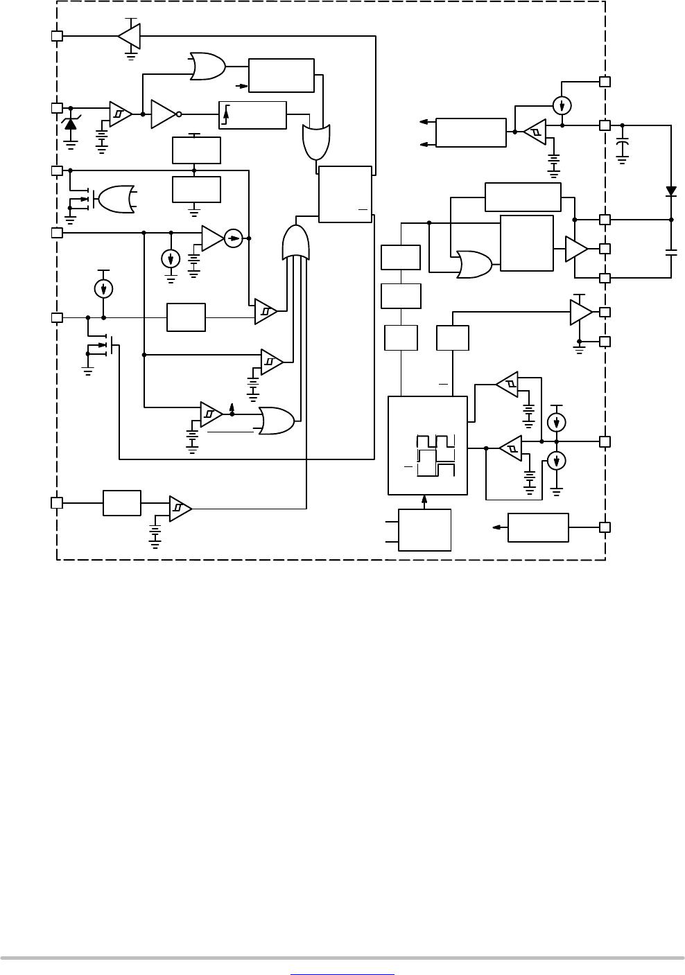
Table 1. PIN FUNCTION DESCRIPTION
Pin Name Description
1 HV This is the input of the high voltage startup regulator and connects directly to the bulk voltage. A constant cur-
rent source supplies current from this pin to the V
CC
capacitor, eliminating the need for an external startup res-
istor. The charge current is 7.5 mA (typical).
2 OSC A capacitor on this pin adjusts the frequency of the internal oscillator. The oscillator sets the frequency of the
half−bridge controller. Each half−bridge switch operates at half the oscillator frequency. The OSC pin also
serves as a disable input for the half−bridge stage. The half−bridge stage is disabled by pulling down this pin
below its disable threshold, V
HB(DIS)
, typically 1.955 V.
3 GND Analog ground.
4 VREF Reference voltage. The capacitor on this pin decouples the internal reference. A 0.1 mF capacitor needs to be
connected between this pin and ground.
5 PFB PFC voltage feedback input. Connect to PFC output using a resistive divider network. The voltage on this pin is
compared to a 2.5 V reference (typical) to regulate the PFC output voltage. The voltage on this pin is also used
to detect PFC undervoltage and overvoltage conditions. In the typical intended application, the PFB pin voltage
will set an upper bound on the PFC output voltage, while the actual PFC voltage control will be exercised by a
control signal generated on the secondary side to provide accurate LED current/voltage control.
6 PCS PFC regulator current sense input. A voltage ramp proportional to the PFC switch current is applied to this pin.
The current sense threshold, V
PCS(ILIM)
, is typically 0.84 V. A 110 ns (typical) leading edge blanking circuit filters
the current sense signal at the start of each cycle.
7 PZCD PFC inductor zero current detector. The inductor current is monitored using an auxiliary winding on the PFC
inductor. The PFC drive signal is enabled during a high to low transition on the PZCD pin. A series resistor limits
the current into the PZCD pin. The watchdog timer is disabled while the PZCD voltage is above the ZCD arming
threshold, V
ZCD(high)
. It is re−enabled once the voltage drops below the ZCD trigger threshold, V
ZCD(low)
. This
feature can be used to disable PFC drive pulses.
8 PControl PFC control voltage. This pin connects to the output of the PFC error amplifier. The error amplifier is a transcon-
ductance amplifier. A compensation network between this pin and grounds sets the PFC loop bandwidth. The
PFC control voltage is compared to a level shifted version of V
PCT
to control the PFC duty ratio. In the typical
intended application, the PControl voltage will be controlled by a secondary side control signal through an opto-
coupler. The optocoupler signal is diode ORed to the internally generated PControl signal and the lower of the
two signals dictates the PFC on-time.
9 PCT PFC on time control capacitor. A 270 mA (typical) current source charges a capacitor connected between this
pin and ground. Once the level shifted PCT voltage reaches V
PControl
, the PFC drive signal is disabled and the
PCT capacitor is discharged.
10 VCC Positive input supply. This pin connects to an external capacitor for energy storage. An internal current source
supplies current from HV to this pin. Once the V
CC
voltage reaches V
CC(on)
(15.3 V typical), the current source
turns off and the controller is enabled. The current source turns on once V
CC
falls to V
CC(off)
(9.3 V typical).
During normal operation, power is supplied to the IC via this pin by means of an auxiliary winding.
11 PGND Ground connection for PDRV and HDRVlo. Tie to the power stage return with a short trace.
12 PDRV PFC switch gate drive control signal. The source and sink drive capability is limited to 60 W and 15 W (typical),
respectively. A discrete driver may be needed to drive the external MOSFET.
13 HDRVlo Half−bridge low side switch gate drive control signal. The source and sink drive capability is limited to 75 W and
15 W (typical), respectively. A discrete driver may be needed to drive the half bridge switch.
14 HVS Half−bridge high side driver source connection. This pin connects directly to the bridge terminal and can float up
to 600 V.
15 HDRVhi Half−bridge high side switch gate drive control signal. The source and sink drive capability is limited to 75 W and
15 W (typical), respectively. The supply terminals of the high side driver connect to the HBoost and HVS pins. A
discrete driver may be needed to drive the half bridge switch.
16 HBoost Supply voltage of the high side gate driver. A charge pump generates a bootstrap voltage floating on top of the
HVS voltage. A diode between the VCC and HBoost pins provides a charge path. The bootstrap voltage is V
CC
minus a diode drop.