NCL30051
www.onsemi.com
4
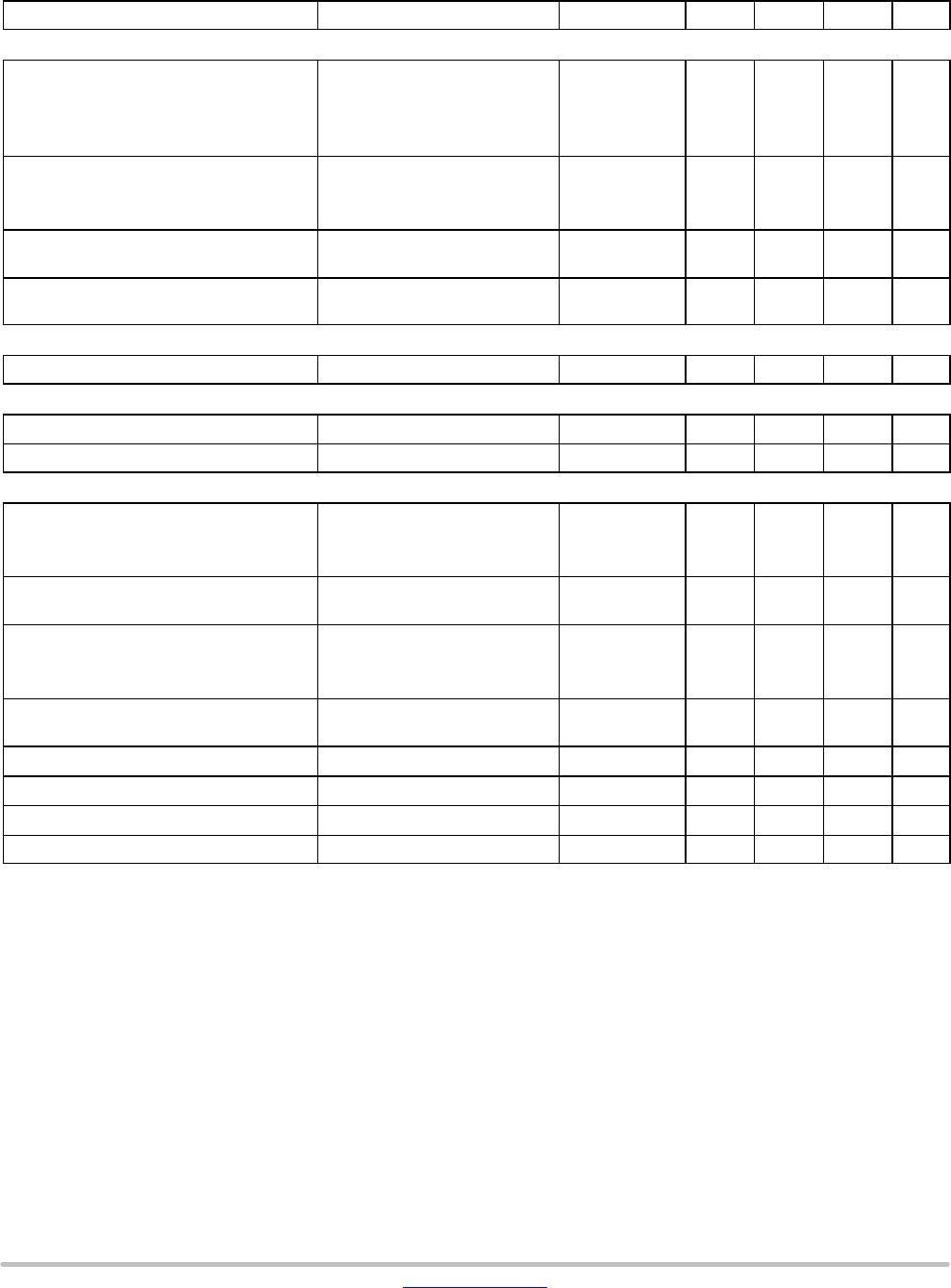
Table 2. MAXIMUM RATINGS (Notes 1 and 2)
Rating Symbol Value Unit
High Voltage Input Voltage V
HV
−0.3 to 600 V
High Voltage Input Current I
HV
10 mA
Supply Input Voltage V
CC
−0.3 to 20 V
Supply Input Current I
CC
10 mA
Oscillator Input Voltage V
OSC
−0.3 to V
REF
V
Oscillator Input Current I
OSC
10 mA
Bandgap Reference Decoupling Output Voltage V
REF
−0.3 to 9 V
Bandgap Reference Decoupling Output Current I
REF
10 mA
PFC Feedback Voltage Input Voltage V
PFB
−0.3 to 10 V
PFC Feedback Voltage Input Current I
PFB
10 mA
PFC Current Sense Input Voltage V
PCS
−0.3 to 10 V
PFC Current Sense Input Current I
PCS
10 mA
PFC Zero Current Detection Input Voltage V
PZCD
−0.3 to 10 V
PFC Zero Current Detection Input Current I
PZCD
10 mA
PFC Control Input Voltage V
PControl
−0.3 to V
REF
V
PFC Control Input Current I
PControl
1.2 mA
PFC On Time Control Input Voltage V
PCT
−0.3 to V
REF
V
PFC On Time Control Input Current I
PCT
9 mA
PFC Drive Signal Voltage V
PDRV
−0.3 to V
CC
V
PFC Drive Signal Current I
PDRV
100 mA
Half−Bridge Low Side Driver Input Voltage V
HDRVlo
−0.3 to V
CC
V
Half−Bridge Low Side Driver Input Current I
HDRVlo
100 mA
Half−Bridge High Side Driver Source Connection Input Voltage V
HVS
−1.0 to 600 V
Half−Bridge High Side Driver Source Connection Input Current I
HVS
100 mA
Half−Bridge High Side Driver Input Voltage V
HDRVhi
−1.3 to V
HVS
+V
CC
V
Half−Bridge High Side Driver Input Current I
HDRVhi
100 mA
Half−Bridge High Side Driver Charge Pump Input Voltage V
HBoost
−0.3 to V
HVS
+V
CC
V
Half−Bridge High Side Driver Charge Pump Input Current I
HBoost
100 mA
High Side Boost Circuit Supply Voltage (between HBoost and HVS pins) V
HBoost(supply)
−0.3 to V
CC
V
High Side Boost Circuit Supply Voltage (between HBoost and HVS pins) I
HBoost(supply)
100 mA
Half−Bridge High Side Driver Source Connection Slew Rate dV
HVS
/dt 50 V/ns
Junction Temperature (Biased) T
J
150 °C
Storage Temperature Range T
stg
–60 to 150 °C
Power Dissipation (T
A
= 25°C, 1 Oz Cu, 0.155 Sq Inch, Printed Circuit Copper Clad)
D Suffix, Plastic Package Case 751B−05 (SOIC−16)
P
D
0.95 W
Thermal Resistance, Junction to Ambient
(1 Oz Cu, 0.155 Sq Inch, Printed Circuit Copper Clad)
D Suffix, Plastic Package Case 751B−05 (SOIC−16)
R
θ
JA
130 °C/W
Stresses exceeding those listed in the Maximum Ratings table may damage the device. If any of these limits are exceeded, device functionality
should not be assumed, damage may occur and reliability may be affected.
1. This device(s) contains ESD protection and exceeds the following tests:
Pins 1, 14, 15 and 16 rated to the maximum voltage of the respective pins based on the maximum ratings table.
All Other Pins: Human Body Model 1500 V per JEDEC Standard JESD22−A114E.
All Other Pins: Machine Model 150 V per JEDEC Standard JESD22−A115−A.
2. This device contains Latch−Up protection and exceeds ± 100 mA per JEDEC Standard JESD78.
NCL30051
www.onsemi.com
5
Table 3. ELECTRICAL CHARACTERISTICS (V
HV
= open, V
PFB
= 2.4 V, V
PCS
= 0 V, V
PZCD
= 5 V, V
PControl
= open, V
CC
= 15 V,
V
PDRV
= open, V
HDRVlo
= open, V
HVS
= 0 V, V
HDRVhi
= open, V
HBoost
= 15 V, C
OSC
= 2200 pF, C
VREF
= 0.1 mF, C
PCT
= 1000 pF, for typical
values T
J
= 25°C, for min/max values, T
J
is −40°C to 125°C, unless otherwise noted)
Characteristics Conditions Symbol Min Typ Max Unit
STARTUP AND SUPPLY CIRCUITS
Supply Voltage
Startup Threshold
Minimum Enable Threshold
Minimum Operating Voltage
V
CC
Increasing
V
CC
Decreasing
V
CC
Decreasing
V
CC(on)
V
CC(enable)
V
CC(off)
14.3
13.6
8.5
15.3
14.6
9.3
16.3
15.6
10.0
V
Supply Current
Device Disabled/Fault
Device Switching
V
PFB
= V
PUVP(low)
(Note 3)
I
CC1
I
CC2
0.8
1.8
1.4
2.4
1.8
3.0
mA
Startup Current V
CC
= V
CC
(on)
– 0.2 V,
V
HV
= 50 V
I
start
3.0 7.5 10.5 mA
Startup Circuit Off−State Leakage Current V
HV
= 600 V,
V
CC
= V
CC
(on)
+ 0.2 V
I
HV(off)
15 50 mA
BANDGAP REFERENCE
Reference Voltage C
REF
= 0.1 mF V
REF
6.605 7.000 7.295 V
OSCILLATOR
Half−Bridge Clock Frequency V
HVS
= 50 V f
clock
13.5 15.5 16.5 kHz
Maximum Half−Bridge Clock Frequency C
OSC
= open f
clock(MAX)
75 kHz
PFC ERROR AMPLIFIER
PFC Feedback Voltage Reference
0°C < T
J
< 125°C
−40°C < T
J
< 125°C
V
PREF
2.42
2.40
2.50
2.58
2.60
V
PFC Feedback Voltage Reference
Regulation with Line
V
CC(on)
+ 0.2 V < V
CC
< 20 V V
PREF(line)
−15 15 mV
Error Amplifier Drive Capability
Sink
Source
V
PControl
= 4 V, V
PFB
= 5 V
V
PControl
= 4 V, V
PFB
= 0.5 V
I
EA(SNK)
I
EA(SRC)
60
−60
80
−80
mA
Open Loop Error Amplifier
Transconductance
V
PControl
= 4 V,
V
PFB
= 2.4 V and 2.6 V
Gm 60 95 mS
Feedback Input Pulldown Current Source V
PFB
= 3 V I
PFB
0.5 1.2 1.5 mA
Error Amplifier Maximum Output Voltage I
PControl
= 10 mA V
EA(OH)
5.30 5.65 6.00 V
Error Amplifier Minimum Output Voltage I
PControl
= −10 mA V
EA(OL)
2.10 2.25 2.40 V
Error Amplifier Output Voltage Range V
EA(OH)
− V
EA(OL)
ΔV
EA
3.1 3.4 3.7 V
3. Resistor/capacitor parallel combination (39 pF || 20 kW) between drive pin and driver supply and between xDRVxx and GND pins.
NCL30051
www.onsemi.com
6
Table 4. ELECTRICAL CHARACTERISTICS (V
HV
= open, V
PFB
= 2.4 V, V
PCS
= 0 V, V
PZCD
= 5 V, V
PControl
= open, V
CC
= 15 V,
V
PDRV
= open, V
HDRVlo
= open, V
HVS
= 0 V, V
HDRVhi
= open, V
HBoost
= 15 V, C
OSC
= 2200 pF, C
VREF
= 0.1 mF, C
PCT
= 1000 pF, for typical
values T
J
= 25°C, for min/max values, T
J
is −40°C to 125°C, unless otherwise noted)
Characteristics Conditions Symbol Min Typ Max Unit
PFC CURRENT SENSE
Current Sense Threshold Voltage
V
PCS(ILIM)
0.78 0.84 0.92 V
Current Sense Input Bias Current V
PCS
= 2 V I
PCS
−1 0 1 mA
Leading Edge Blanking Duration t
PCS(LEB)
40 110 200 ns
Propagation Delay V
PCS
= V
PCS(ILIM)
+ 1 V t
PCS(delay)
90 250 ns
PFC ZERO CURRENT DETECTION
ZCD Threshold Voltage
Arming Threshold
Trigger Threshold
V
PZCD
increasing
V
PZCD
decreasing
V
ZCD(high)
V
ZCD(low)
1.9
1.3
2.1
1.5
2.3
1.7
V
ZCD Voltage Hysteresis V
ZCD(HYS)
400 600 800 mV
ZCD Input Bias Current V
PZCD
= 1 V
V
PZCD
= 5 V
I
PZCD(bias1)
I
PZCD(bias2)
−1
−1
1
1
mA
PFC MAXIMUM OFF TIME
Maximum Off Time t
PFC(off)
50 180 350 ms
PFC ON TIME RAMP GENERATOR
ON time Capacitor Charge Current V
PCT
= 0 V I
PCT(C)
220 270 300 mA
On Time Capacitor Discharge Time V
PCT
= 2.4 V to 0.6 V t
PCT(D)
70 300 ns
ON Time Capacitor Peak Voltage V
PCT(peak)
2.6 3.0 3.4 V
Minimum Duty Ratio V
PFB
= 3.0 V, V
PZCD
= 0 V D
PMIN
0 %
Maximum On Time Detect Delay V
PCT
= V
PCT(peak)
+ 1 V t
PCT(delay)
250 375 ns
Voltage Delta between PControl Voltage
Needed to Generate PDRV Pulses and
V
EA(OL)
DV
EA
− V
PCT(peak)
V
PCT(offset)
250 400 550 mV
PFC OVERVOLTAGE and UNDERVOLTAGE
Overvoltage Detector Threshold Voltage Midpoint between high and low
threshold, V
PControl
= 4 V
V
POVP
1.03*
V
PREF
1.05*
V
PREF
1.07*
V
PREF
V
Overvoltage Comparator Hysteresis Win-
dow
V
PControl
= 4V V
POVP(HYS)
5 30 60 mV
Propagation Delay V
PFB
= V
PREF
+ 1 V t
POVP(delay)
400 800 ns
Undervoltage Detector Threshold Voltage V
PFB
increasing
V
PFB
decreasing
V
PUVP(high)
V
PUVP(low)
175
290
230
350
mV
Undervoltage Comparator Hysteresis V
PFB
increasing V
PUVP(HYS)
20 60 100 mV
PFC DRIVER
PFC Driver Rise Time 10% to 90% (Note 4) t
PDRV(rise)
18 ns
PFC Driver Fall Time 90% to 10% (Note 4) t
PDRV(fall)
9 ns
PFC Driver High State Voltage I
PDRV
= −8 mA V
PDRV(OH)
14.00 14.55 V
PFC Driver Low State Voltage I
PDRV
= 8 mA V
PDRV(OL)
0.12 0.50 V
4. Resistor/capacitor parallel combination (39 pF || 20 kW) between PDRV and driver supply and between PDRV and GND pins.

NCL30051DR2G

Mfr. #:
Manufacturer:
ON Semiconductor
Description:
Power Factor Correction - PFC PFC and Resonant Half Bridge LED Drvr
Lifecycle:
New from this manufacturer.
Delivery:
DHL FedEx Ups TNT EMS
Payment:
T/T Paypal Visa MoneyGram Western Union

Products related to this Datasheet