NCL30051
www.onsemi.com
10
PFC Output Capacitor - Cbulk
The bulk capacitor is one of the most critical components
in the PFC design. High value, high voltage capacitors are
expensive and take up a large space. In traditional PFC
applications, the voltage rating of this capacitor is about
450 V (some designers cut it to 420 V for cost savings), but
for 277 Vac lighting applications, 450 V rating is not
sufficient. As shown in the table above, if the output
voltage is allowed to vary, the bulk voltage can go even
higher. Availability of bulk capacitors above 450 V is
limited. One solution is to take two capacitors and put them
in series. The effective value of two series capacitors is
lower, but for low-medium power applications, this should
not be a big issue. For 600 V maximum bulk voltage, two
400 V capacitors need to be used, but for 90−135 Vac only
applications, lower rated capacitors can be used. When
putting capacitors in series, it is required to have a parallel
high value resistor pair in order to ensure voltage sharing.
The effective bulk capacitance value also depends on the
application requirements. Normal rule of thumb for
traditional PFC circuits is to use around 1 mF/W to achieve
desired hold-up time and ripple performance. In this
approach, due to absence of a regulated second stage, it
may be prudent to increase the capacitance value if low
ripple or fast transient response is required. Another factor
in selecting the capacitor is that it handles high ripple
current due to the CrM topology implemented here. The
equations for ripple current through the capacitor are
derived in ON Semiconductor application note AND8123
and should be used to determine that the selected capacitor
can handle the ripple current without overheating or
lifetime degradation.
PFC Diode (D
BST
)
The PFC diode provides the rectification function and
has to be rated above the peak value of Vbulk. In the CrM
operation, with the diode current going to zero every cycle
prior to its turn-off, the reverse recovery is not that
prominent and an ultrafast diode can be used. In addition,
there is little or no overshoot caused by the reverse
recovery, so the FET voltage is also well contained. In most
cases a 600 V diode is sufficient depending on the derating
criteria.
PFC Switch (Q
BST
)
Typically, the PFC switch is a MOSFET rated anywhere
from 500 V to 650 V. Better commercial availability of
higher voltage rated FETs in recent years has meant that the
QBST is not a major constraint in implementation of
variable Vbulk approach offered by NCL30051. However,
depending on derating guidelines and practices, the 600 V
rating of the FET may not be sufficient. In that case, a
higher voltage FET is required.
PFC Inductor (L
BST
)
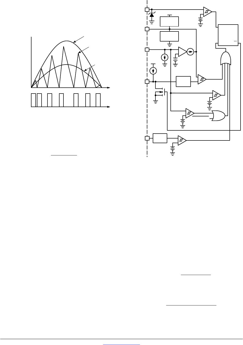
The PFC inductor is designed using the standard CrM
design equations. When the output voltage goes up from
390 V to 540 V, there is about 20% increase in value of
inductance required. Thus, variation in PFC voltage results
in higher boost inductor value and size (and/or higher
ripple current when the output voltage is higher).
HBR Converter Design
The half-bridge resonant converter utilizes an LLC
resonant circuit to achieve the ZVS of the primary switches
and also to reduce the transition losses in the secondary.
Additionally, this circuit offers a major benefit wherein the
output inductor can be eliminated.
In traditional LLC approaches, when the second stage
converter is regulated, the switching frequency of the HBR
converter has to be varied to respond to load or line
changes. As a result, operation near the resonant frequency
is not always guaranteed and the efficiency takes a hit.
Also, varying the frequency imposes additional design
burden on the designer to ensure that the control circuit is
stable and provides desired results over the full load and
line range. The feedback design and loop closure is more
challenging in this type of converter.
By keeping a constant switching frequency, not only is
the control circuit simplified, the magnetics design also
becomes easier. The transformer size can be reduced as it
is designed for a single frequency and full optimization is
available. Studies have shown that this approach leads to
about 25-40% reduction in total magnetics area-product.
Other design considerations for the LLC resonant
converter remain the same as given in ON Semiconductor
application note AND8311 and are not repeated here.
The power conversion architecture of the NCL30051 is
ideal for many LED Lighting applications since it provides
higher efficiency and power factor correction. Since
hold-up time and output ripple are not major considerations
in these applications, NCL30051 fits in very well. This
means that it is ideal for fixed output voltage LED power
supplies (ex: 24 Vdc and 48 Vdc) as well as constant current
schemes where the output voltage varies depending on the
number of LEDs and the variation of the LED forward
voltage. This topology is best suited for applications where
the output voltage variation is constrained to a ratio of
about 1.5 for designs that require operation at 230 Vac.
Supply Sequencing
The error amplifier of the PFC controller is enabled once
V
CC
reaches V
CC(on)
and the PFB voltage exceeds
V
PUVP(high)
, typically 290 mV. Once enabled, the PControl
voltage starts rising and when it exceeds V
EA(OL)
and V
CC
is above V
CC(enable)
, the first PFC drive pulse is generated.
The half-bridge driver is enabled after the first PFC drive
pulse is generated. This ensures a monotonic output
voltage rise as the input voltage to the half bridge stage is
regulated.
In the event that V
CC
falls below V
CC(enable)
before the
control voltage exceeds V
EA(OL)
, the error amplifier will
remain on and V
CC
will fall to Vcc
(OFF)
at which time the
HV startup circuit will be enabled and a new startup
sequence will be initiated.
NCL30051
www.onsemi.com
11
High Voltage Startup Circuit
The NCL30051 internal startup regulator eliminates the
need for external startup components. In addition, this
regulator increases the efficiency of the supply as it uses no
power when in the normal mode of operation, but instead
uses power supplied by an auxiliary winding. The startup
regulator consists of a constant current source that supplies
current from the high voltage line (V
in
) to the supply
capacitor on the V
CC
pin (C
CC
). The startup current (I
start
)
is typically 7.5 mA. The startup circuit is rated at a
maximum voltage of 600 V.
Once C
CC
is charged to 15.3 V (V
CC(on)
), the startup
regulator is disabled and the PFC controller is enabled if the
PFB voltage exceeds V
PUVP(high)
. The startup regulator
remains disabled until the lower supply threshold, V
CC(off)
,
(typically 9.3 V) is reached. Once reached, the drive
outputs are disabled and the startup current source is
enabled. Once the outputs are disabled, the bias current of
the NCL30051 is reduced, allowing V
CC
to charge back up.
The supply capacitor provides power to the controller
while operating in the power up or self−bias mode. During
the converter power up, C
CC
must be sized such that a V
CC
voltage greater than V
CC(off)
is maintained while the
auxiliary supply voltage is building up. Otherwise, V
CC
will collapse and the controller will turn off. The IC bias
current and gate charge load at the drive outputs must be
considered to correctly size C
CC
. The increase in current
consumption due to external gate charge is calculated using
Equation 1.
I
CC(gate charge)
+ f @ Q
G
(eq. 1)
where, f is the operating frequency and Q
G
is the gate
charge of the external MOSFETs.
Main Oscillator
The oscillator frequency is set by the oscillator capacitor,
C
OSC
, on the OSC pin. The oscillator operates at a fixed
80% duty ratio. A current source charges C
OSC
to its peak
voltage, typically 5 V. Once the peak voltage is reached, the
charge current is disabled and C
OSC
is discharged down to
3 V by another current source. The charge and discharge
currents are typically 173 and 692 mA, respectively. The
oscillator frequency vs oscillator capacitance graph is
shown in Figure 3.
Figure 3. Oscillator Frequency vs.
Oscillator Capacitor
C
OSC
, OSCILLATOR CAPACITOR (pF)
2400200016001200400
0
10
30
40
60
70
90
100
f
OSC
, OSCILLATOR FREQUENCY (kHz)
20
50
80
800
An internal clock signal is generated by dividing the
oscillator frequency by two. This clock signal is used to
control the half−bridge driver. The half−bridge duty ratio
is limited to 50%. The PFC is not synchronized to the
oscillator as it operates in variable frequency mode.
Half−Bridge Disable
The half−bridge oscillator and the half−bridge low and
high side drivers are disabled once the voltage on the OSC
pin is brought below the half−bridge disable threshold,
V
HB(DIS)
(typically 1.955 V). This can be accomplished by
pulling down on the oscillator pin using a transistor or open
collector/drain device. Once the oscillator pin is released
the oscillator capacitor returns to its normal operating
range and the half bridge is re−enabled. The low side
half−bridge driver generates the first drive pulse during
initial power up or re−starting of the half−bridge. This
ensures boost voltage is generated to supply the high side
driver.
Voltage Reference
The internal voltage reference, V
REF
, is brought out of
the controller to ease compensation requirements. The
reference voltage is typically 7.0 V. A 0.1 mF bypass
capacitor is required for stability. The reference should not
be loaded with external circuitry.
NCL30051
www.onsemi.com
12
PFC Regulator
The PFC inductor current, I
L(t)
, reaches zero at the end
of the switch cycle as shown in Figure 4 and the average
input current, I
in(t)
, is in phase with the ac line voltage,
V
in(t)
.
Figure 4. Inductor Current in CrM
PFC MOSFET
Drive Signal
I
in
(t)
I
L
(t)
V
in
(t)
t
t
High power factor is achieved in CrM by maintaining a
constant on time (t
on
) for a given RMS input voltage
(V
ac(RMS)
) and load conditions. Equation 2 shows the
relationship between on time and system operating
conditions.
t
on
+
2 @ P
out
@ L
h @ V
ac(RMS)
2
(eq. 2)
where, P
out
is the output power, L is the PFC inductor
inductance and h is the system efficiency.
On Time Control
The NCL30051 controls the on time by charging an
external timing capacitor on the PCT pin, C
T
, with a
constant current source, I
PCT(C)
. The C
T
ramp is then
compared to the control voltage, V
PControl
. The control
voltage is constant for a given RMS line voltage and output
load, satisfying Equation 2. The block diagram of the
constant on time section is shown in Figure 5.
Figure 5. Constant On Time Control Block Diagram
Error
Amplifier
+
+
PFB
Level
Shifter
+
+
+
PFC OVP
Comparator
On time
Comparator
+
+
ZCD
Comparator
PFCoff
PZCD
PCS
LEB
+
Clamp
> 5.65 V
Clamp
PCS
Comparator
+
+
PFC UVP
Comparator
+
V
DD
< 2.25 V
V
DD
V
PREF
I
PCT(C)
V
POVP
V
PUVP
S
R
Q
Dominant
Reset
Latch
Q
V
ZCD
V
CC
Good
PCT
PFC
V
PCS(ILIM)
I
PFB
PControl
10V
The PControl voltage is internally clamped between
2.25 V and 5.65 V. A voltage offset, V
PCT(offset)
, is added
to the C
T
ramp to account for the control voltage range.
This allows the PFC stage to stop the drive pulses (0% duty
ratio) and regulate at light loads. The delta between the
PControl voltage needed to generate a PDRV pulse and the
minimum PControl Clamp voltage is V
PCT(offset)
.
The timing capacitor is discharged and held low once the
C
T
ramp voltage plus offset reaches V
PControl
. The PFC
drive pulse terminates once the C
T
voltage reaches its peak
voltage threshold, V
PCT(peak)
. A new cycle starts once the
inductor current reaches zero detected by a transition on the
ZCD pin or the maximum off time has been reached.
The timing capacitor is sized such that the C
T
ramp peak
voltage is reached at low line and full load. In this operating
mode V
PControl
is at its maximum. Equation 3 is used to
calculate the on time for a given C
T
.
t
on(MAX)
+
C
T
@ V
PCT(peak)
I
PCT(C)
(eq. 3)
Substituting t
on
in Equation 2 with Equation 3 and
rearranging Equation 4 provides a maximum value for C
T
.
C
T
w
2 @ P
out
@ L @ I
PCT(C)
h @ V
ac(RMS)
2
@ V
PCT(peak)
(eq. 4)
where, V
PCT(peak)
, is the maximum PCT voltage, typically
3.0 V.

NCL30051DR2G

Mfr. #:
Manufacturer:
ON Semiconductor
Description:
Power Factor Correction - PFC PFC and Resonant Half Bridge LED Drvr
Lifecycle:
New from this manufacturer.
Delivery:
DHL FedEx Ups TNT EMS
Payment:
T/T Paypal Visa MoneyGram Western Union

Products related to this Datasheet