NCL30051
www.onsemi.com
13
PFC Startup
The output of the error amplifier is pulled low with an
internal pull down transistor when the supply voltage has
not reached V
CC(on)
or if there is a PFC undervoltage fault.
This ensures a soft−start sequence once the PFC is enabled
and eliminates output voltage overshoot during on/off
tests. Once the error amplifier is enabled the output of the
error amplifier charges quickly to the minimum clamp
voltage.
Off Time Control
The PFC off time varies with the instantaneous line
voltage and it is adjusted every cycle to allow the inductor
current to reach zero before the next switch cycle begins.
The inductor is demagnetized once its current reaches zero.
Once the inductor is demagnetized the drain voltage of the
PFC switch begins to drop. The inductor demagnetization
is detected by sensing the voltage across the inductor using
an auxiliary winding. This winding is commonly known as
a zero crossing detector (ZCD) winding. This winding
provides a scaled version of the inductor voltage. Figure 6
shows the ZCD winding arrangement.
Figure 6. ZCD Winding Implementation
PZCD
PFC
Drive
Signal
+
PFC
Output
Voltage
+
Rectified
ac line
voltage
+
V
ZCD
M1
R
PZCD
A negative voltage appears on the ZCD winding while
the PFC switch is on. The PZCD voltage is positive while
the PFC switch is off and current is flowing through the
inductor. The PZCD voltage drops to and rings around zero
volts once the inductor is demagnetized. Once a negative
transition is detected in the PZCD pin the next switch cycle
commences. A positive transition (corresponding to the
PFC switch turn off) arms the ZCD detector to prevent false
triggering. The arming of the ZCD detector is typically
2.1 V (V
PZCD
increasing) and the triggering is typically
1.5 V (V
PZCD
decreasing).
The PZCD pin is internally clamped to 10 V with a zener
diode. A resistor in series with the ZCD pin is required to
limit the current into the PZCD pin. The zener diode
prevents the voltage from exceeding the 10 V clamp or
going below ground. Figure 7 shows typical ZCD
waveforms.
Figure 7. ZCD Winding Waveforms
10 V
0 V
V
ZCD(hig
h)
V
ZCD(low
)
PDRV
Drain
Voltage of
P
FC Switch
V
PZCD
During startup there are no ZCD transitions to enable the
PFC switch. A watchdog timer enables the PFC controller
if no switch pulses are detected for a period of 180 ms
(typical). The watchdog timer is also useful while
operating at light load because the amplitude of the ZCD
signal may be very small to cross the ZCD thresholds. The
watchdog timer is reset at the beginning of a PFC drive
pulse and in a PFC undervoltage fault.
The watchdog timer is disabled if the voltage on the
PZCD pin is above V
ZCD(high)
. It is re−enabled once the
voltage on the PZCD pin drops below V
ZCD(low)
. Disabling
the watchdog timer allows the PFC to be disabled by
pulling up on the PZCD pin. Care should be taken to limit
the current into the PZCD pin to prevent exceeding the
internal 10 V zener clamp.
PFC Compensation
A transconductance error amplifier regulates the PFC
output voltage, Vbulk, by comparing the PFC feedback
signal to an internal 2.5 V reference. As shown in Figure 8
a resistor divider from the PFC output voltage consisting of
R1 and R2 generates the PFC feedback signal.
PFC Error
Amplifier
+
+
PFB
R1
R2
Figure 8. PFC Voltage Sensing
Vbulk
V
PREF
I
PFB
The feedback signal is applied to the amplifier inverting
input. The internal 2.5 V reference, V
PREF
, is applied to the
amplifier non−inverting input. The reference is trimmed
during manufacturing to achieve an accuracy of ±3.2%.
Figure 8 shows the PFC error amplifier and sensing
network. Equation 5 is used to calculate the values of the
PFC feedback network.
NCL30051
www.onsemi.com
14
V
PFC
+ V
PREF
@
R
1
) R
2
R
2
) I
PFB
@ R
1
(eq. 5)
A transconductance amplifier has a voltage−to−current
gain, gm. That is, the output current is controlled by the
differential input voltage. The NCL30051 amplifier has a
typical gm of 95 mS. The PControl pin provides access to the
amplifier output for compensation. The compensation
network is ground referenced allowing the PFC feedback
signal to be used to detect an overvoltage condition.
The compensation network on the PControl pin is
selected to filter the bulk voltage ripple such that a constant
control voltage is maintained across the ac line cycle. A
capacitor between the PControl pin and ground sets a pole.
A pole at or below 20 Hz is enough to filter the ripple
voltage for a 50 and 60 Hz system. The low frequency pole,
f
p
, of the system is calculated using Equation 6.
f
p
+
gm
2pC
PControl
(eq. 6)
where, C
PControl
is the capacitor on the PControl pin to
ground.
A key feature to using a transconductance type amplifier,
is that the input is allowed to move independently with respect
to the output, since the compensation capacitor is connected
to ground. This allows dual usage of the feedback pin by the
error amplifier and by the overvoltage comparator.
PFC Undervoltage
The NCL30051 safely disables the controller if the PFB
pin is left open. An undervoltage detector disables the
controller if the voltage on the PFB pin is below
V
PUVP(low)
, typically 0.23 V. A 1.2 mA (typical) pull down
current source, I
PFB
, ensures V
PFB
falls below V
PUVP(low)
if the PFB pin is floating. The PFB pull down current source
affects the PFC output voltage regulation setpoint.
PFC Overvoltage
An overvoltage detector monitors the PFC feedback
voltage and disables the PFC driver if an overvoltage
condition is detected. This is set internal to the IC at 5%
above the nominal setting of the PFC voltage If an OVP
event is detected, drive pulses are suppressed until the over
voltage condition is removed. The overvoltage detector
tolerance is better than ±2%. The overvoltage detector
threshold, V
POVP
, is the midpoint between the PFC driver
disable and enable thresholds. The overvoltage comparator
hysteresis is the voltage difference between the disable and
enable thresholds. An overvoltage condition is detected
once V
PFB
exceeds V
POVP
by half of V
POVP(HYS)
. The
controller is re-enabled once V
PFB
drops below V
POVP
by
half of V
POVP(HYS)
.
PFC Overcurrent
The PFC current is monitored by means of an overcurrent
detector. The PCS pin provides access to the overcurrent
detector. The PFC drive pulse is terminated if the voltage
on the PCS pin exceeds the overcurrent threshold,
V
PCS(ILIM)
. This comparison is done on a cycle by cycle
basis. The overcurrent threshold is typically 0.84 V.
The current sense signal is prone to leading edge spikes
caused by the power switch transitions. The NCL30051 has
leading edge blanking circuitry that blocks out the first
110 ns (typical) of each current pulse.
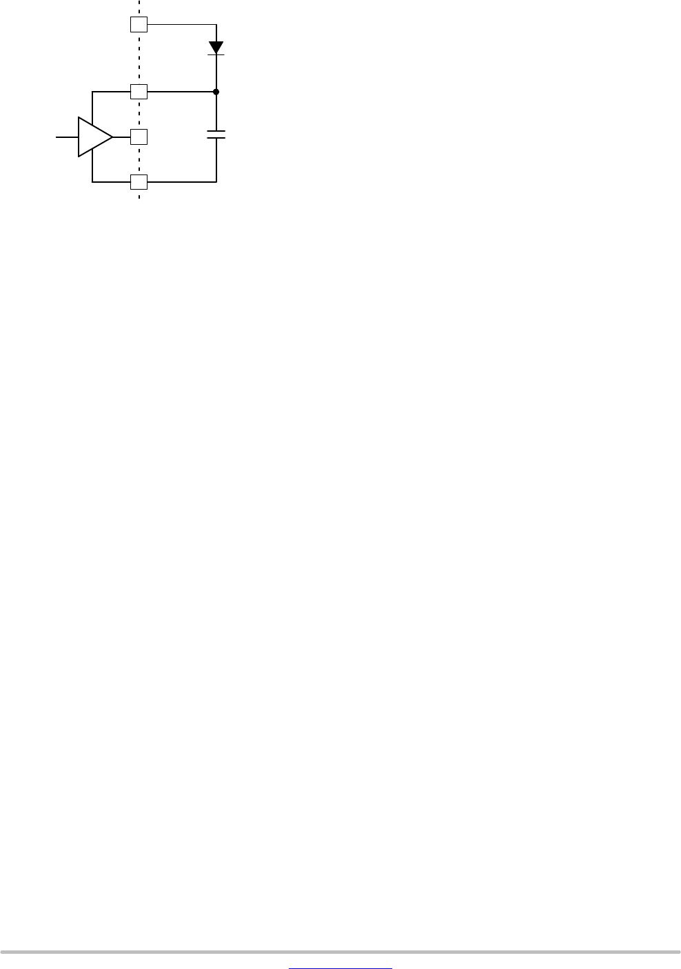
PFC Driver
The PFC driver source and sink impedances are typically
60 and 15 W, respectively. Depending on the external
MOSFET gate charge requirements, an external driver may
be needed to drive the PFC power switch. A driver such as
the one shown in Figure 9 can be easily implemented using
small bipolar transistors.
Figure 9. External Driver
To gate
of MOSFET
VCC
xDRVx
Half−Bridge Driver
The half−bridge stage operates at a fixed 50% duty ratio.
The oscillator frequency is divided by two before it is
applied to the half−bridge controller.
The half−bridge controller has a low side driver,
HDRVlo, and a 600 V high side driver, HDRVhi. The built
in high voltage driver eliminates the need for an external
transformer or dedicated driver. A built−in delay between
each drive transition eliminates the risk of cross
conduction. The delay is typically 785 ns. The typical duty
ratio of each half−bridge driver is 48%.
The high side driver is connected between the HBoost
and the HVS pins as shown in Figure 10.
NCL30051
www.onsemi.com
15
Figure 10. Half−bridge High Side Driver
HVS
HDRVhi
HBoost
VCC
C
boost
D
boost
A boost circuit comprised of D
boost
and C
boost
generates
the supply voltage for the high side driver. Once HDRVlo
turns on, the HVS pin is effectively grounded through the
external power switch. This allows C
boost
to charge to V
CC
.
Once HDRVlo turns off, HVS floats high and D
boost
is
reversed biased. An undervoltage detector monitors the
HBoost voltage. Once the HBoost voltage is greater than
V
Boost(UV)
, typically, 6.1 V, the high side driver is enabled.
The low side driver generally starts before the high side
driver because the boost voltage is generated by the low
side driver switch transitions.
The half−bridge low side driver source and sink
impedances are typically 75 and 15 W, respectively. The
half−bridge high side driver source and sink impedances
are typically 75 and 15 W, respectively. Depending on the
external MOSFETs gate charge requirements, an external
driver may be needed to drive the low and high side power
switches.
Analog and Power Ground
The NCL30051 has an analog ground, GND, and a power
ground, PGND, terminal. GND is used for analog
connections such as VREF and OSC. PGND is used for
high current connections such as the gate drivers. It is
recommended to have independent analog and power
ground planes and connect them at a single point,
preferably at the ground terminal of the system. This will
prevent high current flowing on PGND from injecting
noise in GND. The PGND connection should be as short
and wide as possible to reduce inductance−induced spikes.

NCL30051DR2G

Mfr. #:
Manufacturer:
ON Semiconductor
Description:
Power Factor Correction - PFC PFC and Resonant Half Bridge LED Drvr
Lifecycle:
New from this manufacturer.
Delivery:
DHL FedEx Ups TNT EMS
Payment:
T/T Paypal Visa MoneyGram Western Union

Products related to this Datasheet