LTC4359
6
Rev D
For more information www.analog.com
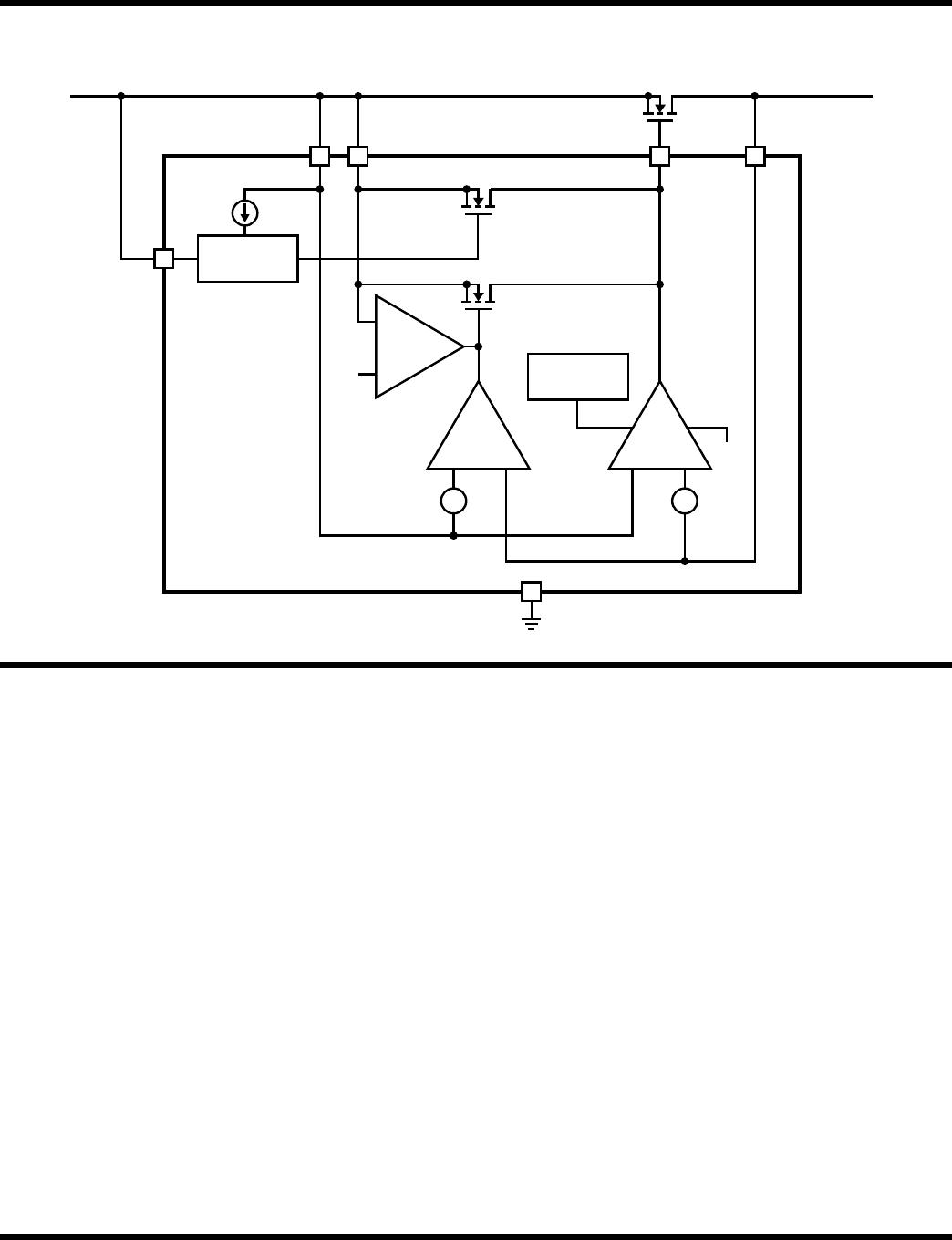
BLOCK DIAGRAM
OPERATION
The LTC4359 controls an external N-channel MOSFET to
form an ideal diode. The GATE amplifier (see Block Dia-
gram) senses across IN and OUT and drives the gate of the
MOSFET to regulate the for
ward voltage to 30mV. As the
load current increases, GATE is driven higher until a point
is reached where the MOSFET is fully on. Further increases
in load current result in a forward drop of R
DS(ON)
• I
LOAD
.
If the load current is reduced, the GATE amplifier drives
the MOSFET gate lower to maintain a 30mV drop. If the
input voltage is reduced to a point where a forward drop
of 30mV cannot be supported, the GATE amplifier drives
the MOSFET off.
In the event of a rapid drop in input voltage, such as an
input short-circuit fault or negative-going voltage spike,
reverse current temporarily flows through the MOSFET.
This current is provided by any load capacitance and by
other supplies or batteries that feed the output in diode-
OR applications.
4359 BD
CHARGE PUMP
TYP. 500kHz
SHUTDOWN
–
+
–
+
FPD
COMP
GATE
AMP
30mV30mV
IN
2.6µA
SOURCE
SHDN
GATE
–1.7V
OUT
V
IN
V
SS
IN
+
–
+
–
–
+
NEGATIVE
COMP
The FPD COMP (Fast Pull-Down Comparator) quickly
responds to this condition by turning the MOSFET off in
300ns, thus minimizing the disturbance to the output bus.
The IN, SOURCE, GATE and SHDN pins are protected
against reverse inputs of up to –40V. The NEGATIVE COMP
detects negative input potentials at the SOURCE pin and
quickly pulls GATE to SOURCE, turning off the MOSFET
and isolating the load from the negative input.
When pulled low the SHDN pin turns off most of the
internal circuitry, reducing the quiescent current to 9µA
and holding the MOSFET off. The SHDN pin may be either
driven high or left open to enable the LTC4359. If left
open, an internal 2.6µA current source pulls SHDN high.
In applications where Q1 is replaced with back-to-back
MOSFETs, the SHDN pin serves as an on/off control for
the forward path, as well as enabling the diode function.