LTC4359
7
Rev D
For more information www.analog.com
Blocking diodes are commonly placed in series with supply
inputs for the purpose of ORing redundant power sources
and protecting against supply reversal. The LTC4359
replaces diodes in these applications with a MOSFET to
reduce both the voltage drop and power loss associated
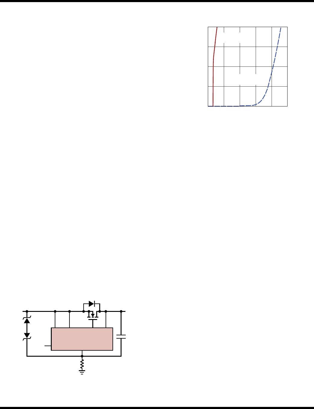
with a passive solution. The curve shown on page 1 illus
-
trates the dramatic improvement in power loss achieved in
a practical application. This represents significant savings
in board area by greatly reducing power dissipation in the
pass device. At low input voltages, the improvement in
forward voltage loss is readily appreciated where head-
room is tight, as shown in Figure2.
The LTC4359 operates from 4V to 80V and withstands
an absolute maximum range of –40V to 100V without
damage. In automotive applications the LTC4359 operates
through load dump, cold crank and two-battery jumps,
and it survives reverse battery connections while also
protecting the load.
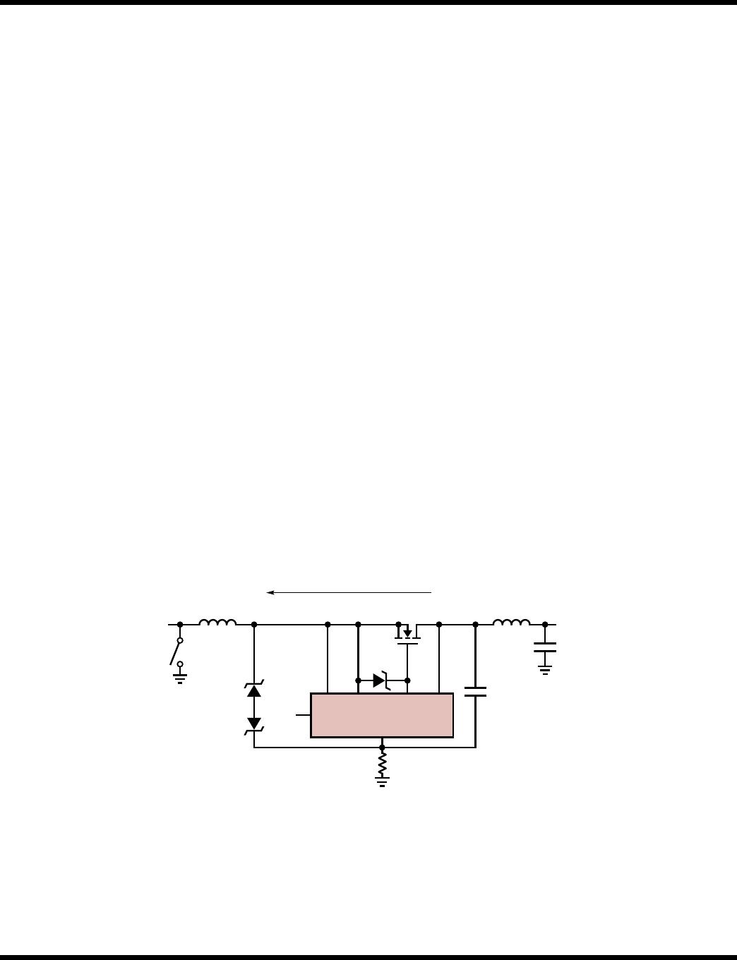
A 12V/20A ideal diode application is shown in Figure1.
Several external components are included in addition to
the MOSFET, Q1. Ideal diodes, like their nonideal coun
-
terparts, exhibit a behavior known as reverse recovery.
In combination with parasitic or intentionally introduced
inductances, reverse recovery spikes may be generated by
an ideal diode during commutation. D1, D2 and R1 protect
against these spikes which might otherwise exceed the
LTC4359’s –40V to 100V survival rating. C
OUT
also plays
a role in absorbing reverse recovery energy. Spikes and
protection schemes are discussed in detail in the Input
Short-Circuit Faults section.
APPLICATIONS INFORMATION
It is important to note that the SHDN pin, while disabling
the LTC4359 and reducing its current consumption to
9µA, does not disconnect the load from the input since
Q1’s body diode is ever-present. A second MOSFET is
required for load switching applications.
MOSFET Selection
All
load current passes through an external MOSFET, Q1.
The important characteristics of the MOSFET are on-
resistance, R
DS(ON)
, the maximum drain-source voltage,
BV
DSS
, and the gate threshold voltage V
GS(TH)
.
Gate drive is compatible with 4.5V logic-level MOSFETs
over the entire operating range of 4V to 80V. In applications
above 8V, standard 10V threshold MOSFETs may be used.
An internal clamp limits the gate drive to 15V maximum
between the GATE and SOURCE pins. For 24V and higher
applications, an external Zener clamp (D4) must be added
between GATE and SOURCE to not exceed the MOSFET’s
V
GS(MAX)
during input shorts.
The maximum allowable drain-source voltage, BV
DSS
, must
be higher than the power supply voltage. If the input is
grounded, the full supply voltage will appear across the
MOSFET. If the input is reversed, and the output is held
up by a charged capacitor, battery or power supply, the
sum of the input and output voltages will appear across
the MOSFET and BV
DSS
> OUT + |V
IN
|.
Figure1. 12V/20A Ideal Diode with Reverse Input Protection
4359 F01
LTC4359
V
SS
SHDN
IN SOURCE
Q1
BSC028N06NS
C
OUT
47nF
R1
1k
GATE
D1
SMAT70A
70V
D2
SMAJ24A
24V
V
IN
12V
V
OUT
12V
20A
OUT
Figure2. Forward Voltage Drop Comparison
Between MOSFET and Schottky Diode
VOLTAGE (V)
0
CURRENT (A)
10
15
0.5
4359 F02
5
0
0.20.1
0.3
0.4
20
MOSFET
(BSC028N06NS)
SCHOTTKY DIODE
(SBG2040CT)
LTC4359
8
Rev D
For more information www.analog.com
APPLICATIONS INFORMATION
The MOSFETs on-resistance, R
DS(ON)
, directly affects
the forward voltage drop and power dissipation. Desired
forward voltage drop should be less than that of a diode
for reduced power dissipation; 100mV is a good starting
point. Choose a MOSFET which has:
R
DS(ON)
<
Forward Voltage Drop
I
LOAD
The resulting power dissipation is
P
d
= (I
LOAD
)
2
• R
DS(ON)
Shutdown Mode
In shutdown, the LTC4359 pulls GATE low to SOURCE,
turning off the MOSFET and reducing its current consump
-
tion to 9µA. Shutdown does not interrupt forward current
flow, a path is still present through Q1’s body diode, as
shown in Figure1. A second MOSFET is needed to block
the forward path; see the section Load Switching and
Inrush Control. When enabled the LTC4359 operates as
an ideal diode. If shutdown is not needed, connect SHDN
to IN. SHDN may be driven with a 3.3V or 5V logic sig
-
nal, or with an open drain or collector. To assert SHDN
low
, the pull down must sink at least 5µA at 500mV. To
enable the part, SHDN must be pulled up to at least 2V.
If SHDN is driven with an open drain, open collector or
switch contact, an internal pull-up current of 2.6µA (1µA
minimum) asserts SHDN high and enables the LTC4359.
If leakage from SHDN to ground cannot be maintained at
less than 100nA, add a pull-up resistor to >2V to assure
turn on. The self-driven open circuit voltage is limited
internally to 2.5V. When floating, the impedance is high
and SHDN is subject to capacitive coupling from nearby
clock lines or traces exhibiting high dV/dt. Bypass SHDN
to V
SS
with 10nF to eliminate injection. Figure 3a is the
simplest way to control the shutdown pin. Since the control
signal ground is different from the SHDN pin reference,
V
SS
, there could be momentary glitches on SHDN during
transients. Figures 3b and 3c are alternative solutions
that level-shift the control signal and eliminate glitches.
Figure 3a. SHDN Control
Figure 3b. Transistor SHDN Control
Figure 4c. Opto-Isolator SHDN Control
4359 F03a
LTC4359
1kVN2222LL
V
SS
SHDN
OFFON
4359 F03b
LTC4359
1k
240k
100k
100k240k
48V
2N5551
V
SS
SHDN
IN
ON
OFF
2N5401
4359 F03c
LTC4359
1k
2MΩ
1MΩ
MOC
207M
2k
48V
V
SS
SHDN
IN
OFFON
Input Short-Circuit Faults
The dynamic behavior of an active, ideal diode entering
reverse bias is most accurately characterized by a delay
followed by a period of reverse recovery. During the delay
phase some reverse current is built up, limited by parasitic
resistances and inductances. During the reverse recovery
LTC4359
9
Rev D
For more information www.analog.com
phase, energy stored in the parasitic inductances is trans-
ferred to other elements in the circuit. Current slew rates
during reverse recovery may reach 100A/µs or higher.
High slew rates coupled with parasitic inductances in
series with the input and output paths may cause poten-
tially destructive transients to appear at the IN, SOURCE
and OUT pins of the LTC4359 during reverse recovery.
A zero impedance short-circuit directly across the input
and ground is especially troublesome because it permits
the highest possible reverse current to build up during
the delay phase. When the MOSFET finally interrupts the
reverse current, the LTC4359 IN and SOURCE pins experi-
ence a negative voltage spike, while the OUT pin spikes in
the positive direction.
T
o prevent damage to the LTC4359 under conditions
of input short-circuit, protect the IN, SOURCE and OUT
pins as shown in Figure4. The IN and SOURCE pins are
protected by clamping to the V
SS
pin with two TransZorbs
or TVS. For input voltages 24V and greater, D4 is needed
to protect the MOSFETs gate oxide during input short-
circuit conditions. Negative spikes, seen after the MOSFET
turns off during an input short, are clamped by D2, a 24V
TVS. D2 allows reverse inputs to 24V while keeping the
MOSFET off and is not required if reverse-input protection
is not needed. D1, a 70V TVS, protects IN and SOURCE in
the positive direction during load steps and overvoltage
conditions. OUT can be protected by an output capacitor,
C
OUT
of at least 1.5µF, a TVS across the MOSFET or by
the MOSFETs avalanche breakdown. Care must be taken
if the MOSFET’s avalanche breakdown is used to protect
the OUT pin. The MOSFETs BV
DSS
must be sufficiently
lower than 100V, and the MOSFETs avalanche energy rat-
ing must be ample enough to absorb the inductive energy.
If a T
VS across the MOSFET or the MOSFET avalanche
is used to protect the OUT pin, C
OUT
can be reduced to
47nF. C
OUT
and R1 preserve the fast turn off time when
output parasitic inductance causes the IN and OUT volt-
ages to drop quickly.
Reverse Input Protection
In the case of a reverse input where negative voltage is
present on the input, the components
D1, D2 and R1
protect the LTC4359. With reverse inputs more negative
than D2’s breakdown voltage (24V), current flows from
system ground through R1. For applications that must
withstand reverse inputs much greater than –24V such
that R1’s power dissipation is unacceptable, it may be
replaced by a diode. If reverse input protection and fast
turn off time are not required, R1 can be removed and V
SS
connected to system ground.
APPLICATIONS INFORMATION
Figure4. Reverse Recovery Produces Inductive Spikes at the IN, SOURCE and OUT Pins.
The Polarity of Step Recovery Is Shown Across Parasitic Inductances
4359 F04
LTC4359
V
SS
SHDN
IN SOURCE OUT
R1
1k
GATE
Q1
FDMS86101
REVERSE RECOVERY CURRENT
INPUT PARASITIC
INDUCTANCE
+
D4
DDZ9699T
12V
V
IN
V
OUT
C
OUT
≥1.5µF
C
LOAD
INPUT
SHORT
OUTPUT PARASITIC
INDUCTANCE
+
D1
SMAT70A
70V
D2
SMAJ24A
24V

LTC4359IMS8#PBF

Mfr. #:
Manufacturer:
Analog Devices / Linear Technology
Description:
Power Management Specialized - PMIC Ideal Diode Cntr w/ Reverse In Prot
Lifecycle:
New from this manufacturer.
Delivery:
DHL FedEx Ups TNT EMS
Payment:
T/T Paypal Visa MoneyGram Western Union