General Description
The MAX7057 frequency-programmable UHF transmit-
ter is designed to transmit ASK/FSK data at a wide
range of frequencies from 300MHz to 450MHz. The
MAX7057 has internal tuning capacitors at the output of
the power amplifier that are programmable for match-
ing to an antenna or load. This allows the user to
change to a new frequency and match the antenna at
the new frequency simultaneously. The MAX7057 trans-
mits at a data rate up to 100kbps nonreturn-to-zero
(NRZ) (50kbps Manchester coded). Typical transmitted
power into a 50 load is +9.2dBm with a +2.7V supply.
The device operates from +2.1V to +3.6V and typically
draws under 12.5mA of current in FSK mode (8.5mA in
ASK mode) when the antenna-matching network is
designed to operate over the 315MHz to 433.92MHz
frequency range. For narrower operating frequency
ranges, the matching network can be redesigned to
improve efficiency. The standby current is less than
1µA at room temperature.
The MAX7057 reference frequency from the crystal
oscillator is multiplied by a fully integrated fractional-N
phase-locked loop (PLL). The multiplying factor of the
PLL is set by a 16-bit number, with 4 bits for integer
and 12 bits for fraction; the multiplying factor can be
anywhere between 19 and 28. The 12-bit fraction in the
synthesizer sets a tuning resolution equal to the refer-
ence frequency divided by 4096; frequency deviation
can be set as low as ±2kHz and as high as ±100kHz.
The fractional-N synthesizer eliminates the problems
associated with oscillator-pulling FSK signal generation.
The MAX7057 has a serial peripheral interface (SPI™)
for selecting all the necessary settings.
The MAX7057 is available in a 16-pin SO package and
is specified to operate in the -40°C to +125°C automo-
tive temperature range.
Applications
RF Remote Controls
Garage Door Openers
Home Automation
Automotive
Wireless Sensors
Wireless Game Consoles
Wireless Computer Peripherals
Security Systems
Features
o Programmable Frequency Operation with Single
Crystal
o Internal Variable Capacitor for Antenna Tuning
with Single-Matching Network
o 100kbps Data Rate (NRZ)
o +2.1V to +3.6V Single-Supply Operation
o < 12.5mA (FSK), < 8.5mA (ASK) DC Current Drain
o < 1µA Standby Current
o ASK/FSK Modulation
o 47% Carrier Tuning Range Using One Crystal
MAX7057
300MHz to 450MHz Frequency-Programmable
ASK/FSK Transmitter
________________________________________________________________
Maxim Integrated Products
1
Pin Configuration
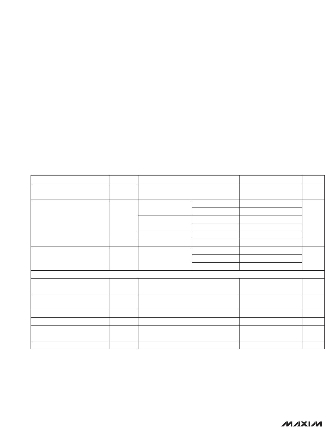
Ordering Information
19-4093; Rev 1; 4/11
For pricing, delivery, and ordering information, please contact Maxim Direct at 1-888-629-4642,
or visit Maxim’s website at www.maxim-ic.com.
EVALUATION KIT
AVAILABLE
+
Denotes a lead(Pb)-free package/RoHs-compliant package.
PART TEMP RANGE PIN-PACKAGE
MAX7057ASE+ -40°C to +125°C 16 SO
Typical Application Circuit and Functional Diagram appear
at end of data sheet.
SPI is a trademark of Motorola, Inc.
DGND
DINPAGND
1
+
2
DVDD
GPOSDI
SCLK
CS
TOP VIEW
3
4
AGND
XTAL1
XTAL2
PAVDD
AVDD
5 ENABLEPAOUT
ROUT 6
7
8
MAX7057
14
13
16
15
12
11
10
9
MAX7057
300MHz to 450MHz Frequency-Programmable
ASK/FSK Transmitter
2 _______________________________________________________________________________________
ABSOLUTE MAXIMUM RATINGS
DC ELECTRICAL CHARACTERISTICS
(
Typical Application Circuit
, 50 system impedance, tuned for 315MHz to 433.92MHz operation, V
AVDD
= V
DVDD
= V
PAVDD
= +2.1V
to +3.6V, f
RF
= 300MHz to 450MHz, f
CRYSTAL
= 16MHz, T
A
= -40°C to +125°C, unless otherwise noted. Typical values are at V
AVDD
= V
DVDD
= V
PAVDD
= +2.7V, T
A
= +25°C, unless otherwise noted. All min and max values are 100% tested at T
A
= +125°C, and
guaranteed by design and characterization over temperature, unless otherwise noted.)
Stresses beyond those listed under “Absolute Maximum Ratings” may cause permanent damage to the device. These are stress ratings only, and functional
operation of the device at these or any other conditions beyond those indicated in the operational sections of the specifications is not implied. Exposure to
absolute maximum rating conditions for extended periods may affect device reliability.
Supply Voltage, PAVDD, AVDD, DVDD to AGND,
DGND, PAGND ...................................................-0.3V to +4.0V
All Other Pins..................................._GND - 0.3V to _V
DD
+ 0.3V
Continuous Power Dissipation (T
A
= +70°C)
16-Pin SO (derate 8.7mW/°C above +70°C)...............695.7mW
Operating Temperature .....................................-40°C to +125°C
Storage Temperature Range .............................-65°C to +150°C
Lead Temperature (soldering, 10s) .................................+300°C
Soldering Temperature (reflow) .......................................+260°C
PARAMETER SYMBOL CONDITIONS MIN TYP MAX UNITS
Supply Voltage V
DD
PAVDD, AVDD, and DVDD connected to
power supply, V
DD
2.1 2.7 3.6 V
f
RF
= 315MHz 3.9 6.5
PA off, V
DIN
at 0%
duty cycle (ASK)
f
RF
= 433.92MHz 4.5 7.5
f
RF
= 315MHz 8.1 15.1
V
D IN
at 50% d uty cycl e
( AS K) ( N otes 1, 2, 3)
f
RF
= 433.92MHz 8.5 15.0
f
RF
= 315MHz 12.2 23.7
Supply Current I
DD
V
DIN
at 100% duty
cycle (FSK) (Note 1)
f
RF
= 433.92MHz 12.4 22.4
mA
T
A
= + 25°C ( N ote 3) 0.8
T
A
< + 85°C ( N ote 3) 1 6.4Standby Current I
STDBY
V
ENABLE
< V
IL
T
A
< +125°C 6.2 20.1
µA
DIGITAL I/O
Input High Threshold V
IH
0.9 x
V
DVDD
V
Input Low Threshold V
IL
0.1 x
DV
DD
V
Input Pulldown Sink Current 13 µA
Input Pullup Source Current A
Output-Voltage High V
OH
I
SINK
= 500µA (GPO)
V
DD
-
0.37
V
Output-Voltage Low V
OL
I
SOURCE
= 500µA (GPO) 0.36 V
MAX7057
300MHz to 450MHz Frequency-Programmable
ASK/FSK Transmitter
_______________________________________________________________________________________ 3
AC ELECTRICAL CHARACTERISTICS
(
Typical Application Circuit
, 50 system impedance, tuned for 315MHz to 433.92MHz operation, V
AVDD
= V
DVDD
= V
PAVDD
= +2.1V
to +3.6V, f
RF
= 300MHz to 450MHz, f
CRYSTAL
= 16MHz, T
A
= -40°C to +125°C, unless otherwise noted. Typical values are at V
AVDD
= V
DVDD
= V
PAVDD
= +2.7V, T
A
= +25°C, unless otherwise noted. All min and max values are 100% tested at T
A
= +125°C, and
guaranteed by design and characterization over temperature, unless otherwise noted.)
PARAMETER SYMBOL CONDITIONS MIN TYP MAX UNITS
GENERAL CHARACTERISTICS
Frequency Range 300 450 MHz
ENABLE transition low-to-high, frequency
settled to within 50kHz of the desired carrier
120
Power-On Time t
ON
ENABLE transition low-to-high, frequency
settled to within 5kHz of the desired carrier
260
µs
Manchester encoded 50
ASK mode
Nonreturn-to-Zero 100
Manchester encoded 50
Maximum Data Rate
FSK mode
Nonreturn-to-Zero 100
kbps
Frequency Switching Time
Time from end of SPI write to frequency
settled to within 5kHz of desired carrier
70 µs
PHASE-LOCKED LOOP (PLL)
VCO Gain K
VCO
320 MHz/V
10kHz offset -78
f
RF
= 315MHz
1MHz offset -98
10kHz offset -73
PLL Phase Noise
f
RF
= 433.92MHz
1MHz offset -98
dBc/Hz
Loop Bandwidth 300 kHz
Reference Frequency Input Level 500 mV
P-P
Frequency-Divider Range 19 28
Frequency Deviation (FSK) ±2 ±100 kHz
CRYSTAL OSCILLATOR
Crystal Frequency f
XTAL
10.71 16 23.68 MHz
Frequency Pulling by V
DD
4 ppm/V
Crystal Load Capacitance (Note 4) 10 pF
POWER AMPLIFIER (PA)
T
A
= +25°C (Note 3) 3.8 9.2 16.4
T
A
= +125°C, V
AVDD
= V
DVDD
= V
PAVDD
=
+2.1V
2.4 5.2
Output Power (Note 1) P
OUT
T
A
= -40°C, V
AVDD
= V
DVDD
= V
PAVDD
=
+3.6V (Note 3)
12.6 17.0
dBm
Modulation Depth 71 dB
f
RF
= 315MHz -29
Maximum Carrier Harmonics
With output matching
network
f
RF
= 433.92MHz -44
dBc
Reference Spur -45 dBc

MAX7057ASE+

Mfr. #:
Manufacturer:
Maxim Integrated
Description:
RF Transmitter 300-450MHz f-Prog ASK/FSK Transmitter
Lifecycle:
New from this manufacturer.
Delivery:
DHL FedEx Ups TNT EMS
Payment:
T/T Paypal Visa MoneyGram Western Union

Products related to this Datasheet