Using a byte descriptive notation, the reset command
can be viewed as the following sequence, within the
same CS cycle:
SDI: <0x04>
Features and Settings
Values and parameters are set through registers in the
MAX7057 that are addressable through the SPI. These
registers contain bits that either turn functions on and
off or program numerical settings. The following set-
tings are controlled through the SPI.
Variable Capacitor
The internal variable shunt capacitor, which is instru-
mental in matching the PA to the antenna, is controlled
by setting 5 bits in the configuration 0 register. This
allows for 32 levels of shunt capacitance control. Since
the control of these 5 bits is independent of the other
settings, any capacitance value can be chosen at any
frequency, making it possible to maintain maximum
transmitter efficiency while moving rapidly from one fre-
quency to another.
Clock Output
The MAX7057 has a buffered clock output that can
serve as a clock for a microprocessor. The divide ratio
is set through the configuration 0 register (see Tables 5
and 6). The divide settings are 1 (no division), 2, 4, 8, or
16; the original undivided frequency is based on the
reference frequency generated by the external crystal.
The buffered clock output is available at GPO when
enabled by setting the configuration 1 register (see
Tables 2, 3, 15, and 16).
Mode Select and Crystal Shutdown
The transmission mode is selected by writing to a regis-
ter. The default mode is ASK and the mode can be
changed to FSK by writing a 1 to the mode bit in the
control register. This register is also used to keep the
crystal circuit powered up in the shutdown mode.
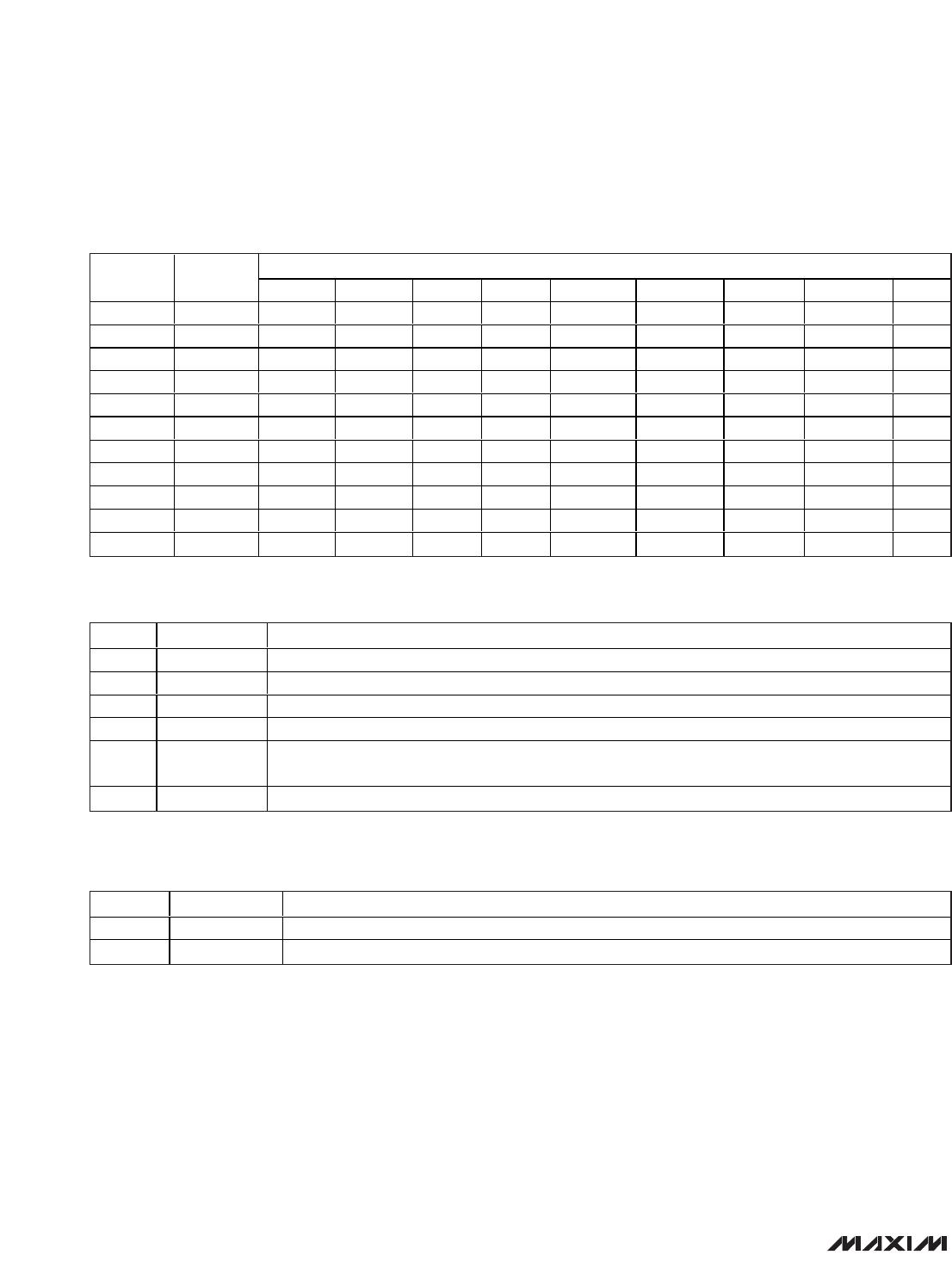
Registers
The following tables provide information on the
MAX7057 registers.
MAX7057
300MHz to 450MHz Frequency-Programmable
ASK/FSK Transmitter
______________________________________________________________________________________ 13
SDI
SCLK
CS
RESET COMMAND (0x04)
ADDRESS REGISTER NAME DESCRIPTION
0x00 CONTRL
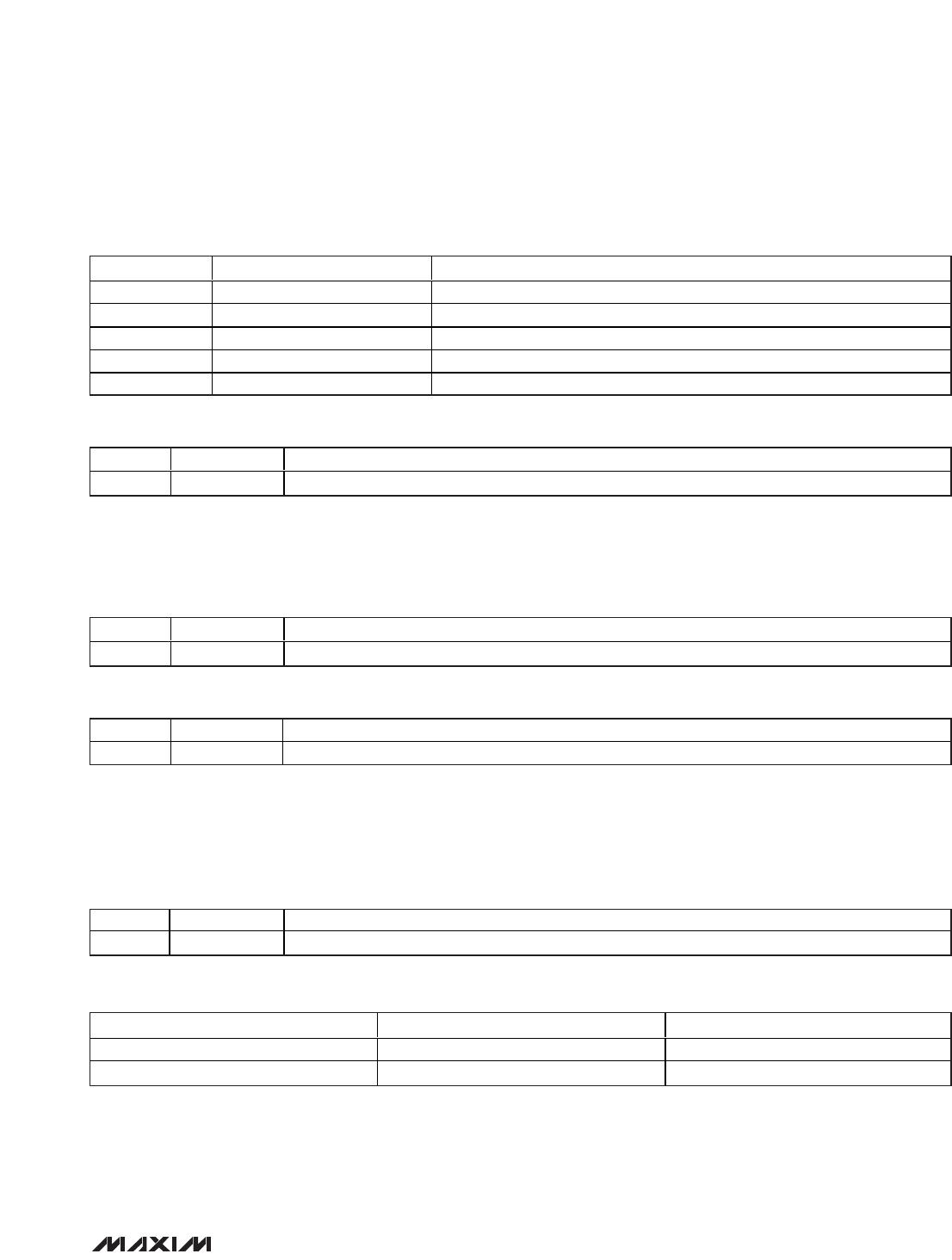
Control register. Controls the mode (ASK/FSK), crystal clock output, envelope-shaping, PLL
bandwidth, and SPI enable.
0x01 CONFIG0
Configuration 0 register. Controls the capacitance at the PA output and clock output
frequency divider.
0x02 HIFREQ1 High-frequency 1 register (upper byte). Sets the high frequency in FSK transmission.
0x03 HIFREQ0 High-frequency 0 register (lower byte). Sets the high frequency in FSK transmission.
0x04 LOFREQ1
Low-frequency 1 register (upper byte). Sets the low frequency in FSK transmission, or
carrier frequency in ASK transmission.
0x05 LOFREQ0
Low-frequency 0 register (lower byte). Sets the low frequency in FSK transmission, or carrier
frequency in ASK transmission.
0x06 FLOAD Frequency load register. Performs the frequency load function.
0x07 DATAIN Data in register. SPI equivalent of DIN pin.
0x08 EN Enable register. SPI equivalent of ENABLE pin.
0x09 CONFIG1 Configuration 1 register. GPO selector.
0x0C STATUS Status register.
Figure 6. Reset Command Format
Table 2. Register Summary
MAX7057
300MHz to 450MHz Frequency-Programmable
ASK/FSK Transmitter
14 ______________________________________________________________________________________
BIT NAME FUNCTION
4-0 cap[4:0] 5-bit capacitor setting
7-5 ckdiv[2:0] 3-bit clock output frequency divider
Table 5. Configuration 0 Register (Address: 0x01)
DATA
NAME ADDRESS
BIT 7 BIT 6 BIT 5 BIT 4 BIT 3 BIT 2 BIT 1 BIT 0 MODE
CONTRL 0x00 0 0 spioffsht pllbw shape ckouts ckouton mode R/W
CONFIG0 0x01 ckdiv[2] ckdiv[1] ckdiv[0] cap[4] cap[3] cap[2] cap[1] cap[0] R/W
HIFREQ1 0x02 fhi[15] fhi[14] fhi[13] fhi[12] fhi[11] fhi[10] fhi[9] fhi[8] R/W
HIFREQ0 0x03 fhi[7] fhi[6] fhi[5] fhi[4] fhi[3] fhi[2] fhi[1] fhi[0] R/W
LOFREQ1 0x04 flo[15] flo[14] flo[13] flo[12] flo[11] flo[10] flo[9] flo[8] R/W
LOFREQ0 0x05 flo[7] flo[6] flo[5] flo[4] flo[3] flo[2] flo[1] flo[0] R/W
FLOAD 0x06 fload R/W
DATAIN 0x07 datain_bit R/W
EN 0x08 enable_bit R/W
CONFIG1 0x09 0 0 0 0 0 gposel[2] gposel[1] gposel[0] R/W
STATUS 0x0C fhi/lo[15] fhi/lo[14] fhi/lo[13] fhi/lo[12] X 0 TxREADY NoXTAL R
Table 3. Register Configuration
BIT NAME FUNCTION
0 mode ASK(0) or FSK(1)
1 ckouton Crystal clock output enable(1) on GPO output
2 ckouts Crystal clock output enable(1) while part is in shutdown mode
3 shape Disable(0) or enable(1) transmitter envelope-shaping resistor
4 pllbw
PLL bandwidth setting, low(0) = 300kHz or high(1) = 600kHz; 300kHz is recommended for fractional-N
and 600kHz for fixed-N
5 spioffsht Enable(0) or disable(1) SPI communication during shutdown
Table 4. Control Register (Address: 0x00)
The 4 MSBs of HIFREQ1 (fhi[15:12]) are the integer
portion of the divider, excluding offset of 16. The 12
LSBs (fhi[11:0]) are the fractional part of the divider.
MAX7057
300MHz to 450MHz Frequency-Programmable
ASK/FSK Transmitter
______________________________________________________________________________________ 15
DECIMAL BINARY CRYSTAL FREQUENCY DIVIDED BY
0 000 1
1 001 2
2 010 4
3 011 8
4-7 1XX 16
Table 6. ckdiv[2:0] of Configuration 0 Register (Address: 0x01)
BIT NAME FUNCTION
7-0 fhi[15:8] 8-bit upper byte of high-frequency divider for FSK
Table 7. High-Frequency 1 Register (Address: 0x02)
BIT NAME FUNCTION
7-0 fhi[7:0] 8-bit lower byte of high-frequency divider for FSK
Table 8. High-Frequency 0 Register (Address: 0x03)
BIT NAME FUNCTION
7-0 flo[15:8] 8-bit upper byte of low-frequency divider for FSK/ASK
Table 9. Low-Frequency 1 Register (Address: 0x04)
BIT NAME FUNCTION
7-0 flo[7:0] 8-bit lower byte of low-frequency divider for FSK/ASK
Table 10. Low-Frequency 0 Register (Address: 0x05)
DECIMAL VALUE fhi[15:12], flo[15:12] fhi[11:0], flo[11:0]
12.0220 0xC 0x05A
2.9536 0x2 0xF42
Table 11. Maximum and Minimum Values for Frequency Divide
The 4 MSBs of LOFREQ1 (flo[15:12]) are the integer
portion of the divider, excluding offset of 16. The 12
LSBs (flo[11:0]) are the fractional part of the divider.
Valid values for the divider are shown in Table 11.

MAX7057ASE+

Mfr. #:
Manufacturer:
Maxim Integrated
Description:
RF Transmitter 300-450MHz f-Prog ASK/FSK Transmitter
Lifecycle:
New from this manufacturer.
Delivery:
DHL FedEx Ups TNT EMS
Payment:
T/T Paypal Visa MoneyGram Western Union

Products related to this Datasheet