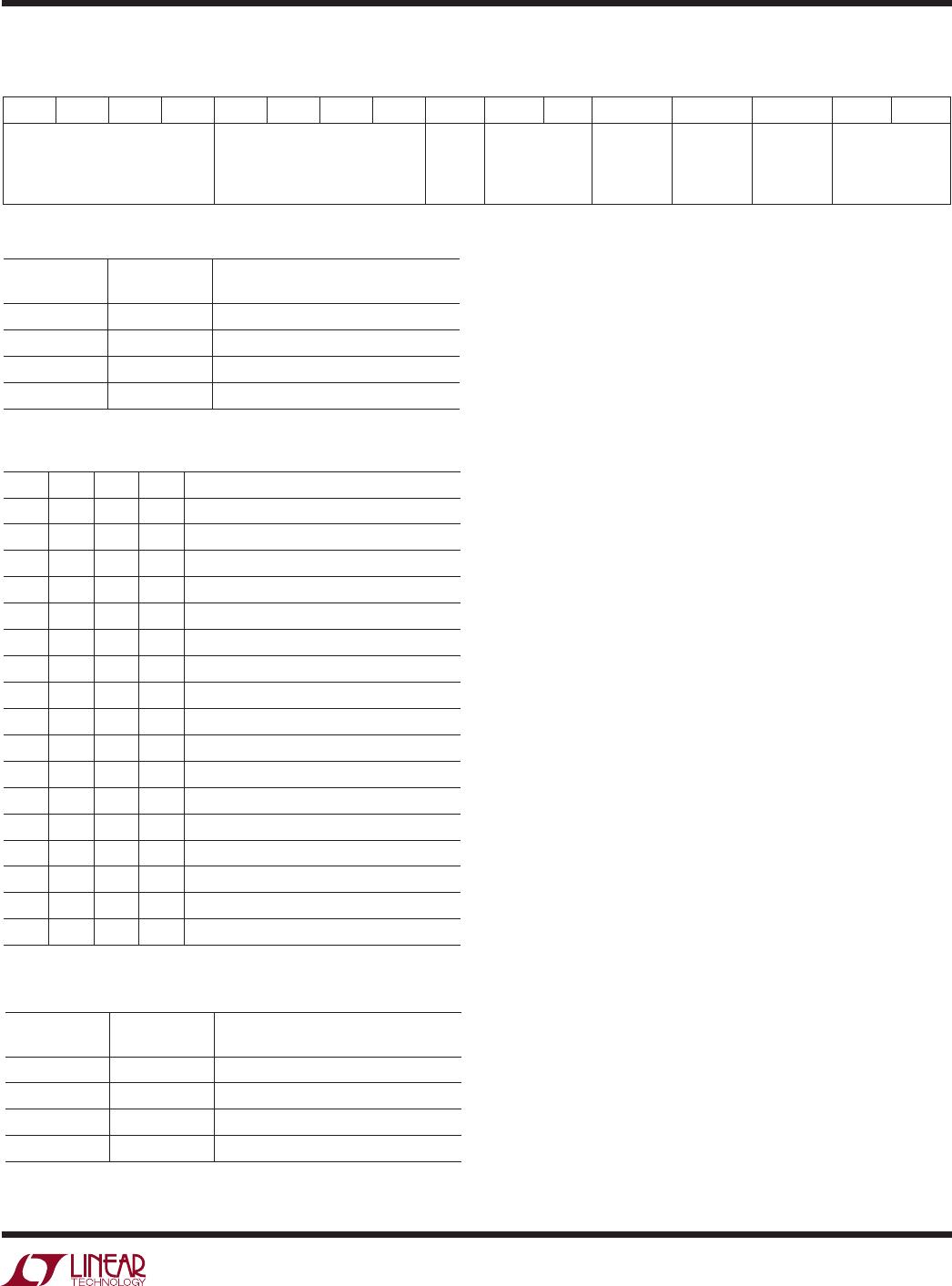
LTC3555/LTC3555-X
19
3555fe
For more information www.linear.com/LTC3555
1022 times the current in the PROG pin. The program
resistor and the charge current are calculated using the
following equations:
R
PROG
=
1022V
I
CHG
, I
CHG
=
1022V
R
PROG
In either the constant-current or constant-voltage charging
modes, the voltage at the PROG pin will be proportional to
the actual charge current delivered to the battery. There-
fore, the actual charge current can be determined at any
time by monitoring the PROG pin voltage and using the
following equation:
I
BAT
=
V
PROG
R
PROG
1022
In many cases, the actual battery charge current, I
BAT
, will
be lower than I
CHG
due to limited input power available
and prioritization with the system load drawn from V
OUT
.
Charge Status Indication
The CHRG pin indicates the status of the battery charger.
Four possible states are represented by CHRG which in-
clude charging, not charging, unresponsive battery, and
battery temperature out of range.
The signal at the CHRG pin can be easily recognized as
one of the above four states by either a human or a mi-
croprocessor. An open-drain output, the CHRG pin can
drive an indicator LED through a current limiting resistor
for human interfacing or simply a pull-up resistor for
microprocessor interfacing.
To make the CHRG pin easily recognized by both humans
and microprocessors, the pin is either low for charging,
high for not charging, or it is switched at high frequency
(35kHz) to indicate the two possible faults, unresponsive
battery and battery temperature out of range.
When charging begins, CHRG is pulled low and remains
low for the duration of a normal charge cycle. When
charging is complete, i.e., the BAT pin reaches the float
voltage and the charge current has dropped to one tenth
of the programmed value, the CHRG pin is released (Hi-Z).
If a fault occurs, the pin is switched at 35kHz. While
switching, its duty cycle is modulated between a low
and high value at a very low frequency. The low and high
duty cycles are disparate enough to make an LED appear
to be on or off thus giving the appearance of “blinking”.
Each of the two faults has its own unique “blink” rate for
human recognition as well as two unique duty cycles for
machine recognition.
The CHRG pin does not respond to the C/10 threshold if
the LTC3555 family is in V
BUS
current limit. This prevents
false end-of-charge indications due to insufficient power
available to the battery charger.
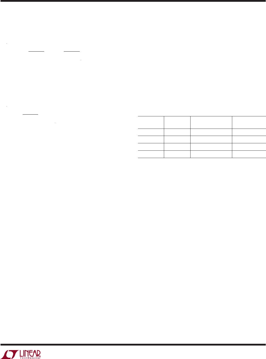
Table 1 illustrates the four possible states of the CHRG
pin when the battery charger is active.
Table 1. CHRG Signal
STATUS
FREQUENCY
MODULATION
(BLINK) FREQUENCY
DUTY CYCLES
Charging 0Hz 0Hz (Lo-Z) 100%
Not Charging 0Hz 0Hz (Hi-Z) 0%
NTC Fault 35kHz 1.5Hz at 50% 6.25% to 93.75%
Bad Battery 35kHz 6.1Hz at 50% 12.5% to 87.5%
An NTC fault is represented by a 35kHz pulse train whose
duty cycle varies between 6.25% and 93.75% at a 1.5Hz
rate. A human will easily recognize the 1.5Hz rate as a
“slow” blinking which indicates the out-of-range battery
temperature while a microprocessor will be able to decode
either the 6.25% or 93.75% duty cycles as an NTC fault.
If a battery is found to be unresponsive to charging (i.e.,
its voltage remains below 2.85V for 1/2 hour), the CHRG
pin gives the battery fault indication. For this fault, a human
would easily recognize the frantic 6.1Hz “fast” blink of the
LED while a microprocessor would be able to decode either
the 12.5% or 87.5% duty cycles as a bad battery fault.
Note that the LTC3555 family is a three terminal PowerPath
product where system load is always prioritized over battery
charging. Due to excessive system load, there may not be
sufficient power to charge the battery beyond the trickle
charge threshold voltage within the bad battery timeout
period. In this case, the battery charger will falsely indicate
a bad battery. System software may then reduce the load
and reset the battery charger to try again.
Although very improbable, it is possible that a duty cycle
reading could be taken at the bright-dim transition (low
duty cycle to high duty cycle). When this happens the
OPERATION
LTC3555/LTC3555-X
20
3555fe
For more information www.linear.com/LTC3555
duty cycle reading will be precisely 50%. If the duty cycle
reading is 50%, system software should disqualify it and
take a new duty cycle reading.
NTC Thermistor
The battery temperature is measured by placing a nega-
tive temperature coefficient (NTC) thermistor close to the
battery pack.
To use this feature, connect the NTC thermistor, R
NTC
,
between the NTC pin and ground and a resistor, R
NOM
,
from V
BUS
to the NTC pin. R
NOM
should be a 1% resistor
with a value equal to the value of the chosen NTC therm-
istor at 25°C (R25). For applications requiring greater
than 750mA of charging current, a 10k NTC thermistor is
recommended due to increased interference.
The LTC3555 family will pause charging when the
resistance of the NTC thermistor drops to 0.54 times
the value of R25 or approximately 5.4k. For a Vishay
Curve 1 thermistor, this corresponds to approximately
40°C. If the battery charger is in constant voltage (float)
mode, the safety timer also pauses until the thermistor
indicates a return to a valid temperature. As the tempera-
ture drops, the resistance of the NTC thermistor rises. The
LTC3555 family is also designed to pause charging when
the value of the NTC thermistor increases to 3.25 times
the value of R25. For Vishay Curve 1 this resistance,
32.5k, corresponds to approximately 0°C. The hot and cold
comparators each have approximately 3°C of hysteresis
to prevent oscillation about the trip point. Grounding the
NTC pin disables the NTC charge pausing function.
Thermal Regulation
To optimize charging time, an internal thermal feedback
loop may automatically decrease the programmed charge
current. This will occur if the die temperature rises to
approximately 110°C. Thermal regulation protects the
LTC3555 family from excessive temperature due to high
power operation or high ambient thermal conditions and
allows the user to push the limits of the power handling
capability with a given circuit board design without risk of
damaging the part or external components. The benefit of
the LTC3555 family thermal regulation loop is that charge
current can be set according to actual conditions rather
than worst-case conditions with the assurance that the
battery charger will automatically reduce the current in
worst-case conditions.
I
2
C Interface
The LTC3555 family may receive commands from a host
(master) using the standard I
2
C 2-wire interface. The Timing
Diagram shows the timing relationship of the signals on
the bus. The two bus lines, SDA and SCL, must be high
when the bus is not in use. External pull-up resistors or
current sources, such as the LTC1694 I
2
C accelerator, are
required on these lines. The LTC3555 family is a receive-
only slave device. The I
2
C control signals, SDA and SCL
are scaled internally to the DV
CC
supply. DV
CC
should be
connected to the same power supply as the microcontroller
generating the I
2
C signals.
The I
2
C port has an undervoltage lockout on the DV
CC
pin. When DV
CC
is below approximately 1V, the I
2
C serial
port is cleared and switching regulators 2 and 3 are set
to full scale.
Bus Speed
The I
2
C port is designed to be operated at speeds of up
to 400kHz. It has built-in timing delays to ensure correct
operation when addressed from an I
2
C compliant master
device. It also contains input filters designed to suppress
glitches should the bus become corrupted.
Start and Stop Conditions
A bus-master signals the beginning of a communication to
a slave device by transmitting a START condition. A START
condition is generated by transitioning SDA from high
to low while SCL is high. When the master has finished
communicating with the slave, it issues a STOP condition
by transitioning SDA from low to high while SCL is high.
Byte Format
Each byte sent to the LTC3555 family must be eight bits
long followed by an extra clock cycle for the acknowledge
bit to be returned by the LTC3555 family. The data should be
sent to the LTC3555 family most significant bit (MSB) first.
OPERATION
LTC3555/LTC3555-X
21
3555fe
For more information www.linear.com/LTC3555
OPERATION
Table 2. I
2
C Serial Port Mapping
A7 A6 A5 A4 A3 A2 A1 A0 B7 B6 B5 B4 B3 B2 B1 B0
Switching Regulator 2
Voltage (See Table 4)
Switching Regulator 3
Voltage (See Table 4)
Disable
Battery
Charger
Switching
Regulator
Modes
(See Table 5)
Enable
Regulator
1
Enable
Regulator
2
Enable
Regulator
3
Input Current
Limit
(See Table 3)
Table 3. USB Current Limit Settings
B1
(I
LIM1
)
B0
(I
LIM0
)
USB SETTING
0 0 1x Mode (USB 100mA Limit)
0 1 10x Mode (Wall 1A Limit)
1 0 Suspend
1 1 5x Mode (USB 500mA Limit)
Table 5. General Purpose Switching Regulator Modes
B6
(SDA)*
B5
(SCL)*
Switching Regulator Mode
0 0 Pulse Skip
0 1 Forced Burst Mode Operation
1 0 LDO Mode
1 1 Burst Mode Operation
*SDA and SCL take on this context only when DV
CC
= 0V.
Table 4. Switching Regulator Servo Voltage
A7 A6 A5 A4 Switching Regulator 2 Servo Voltage
A3 A2 A1 A0 Switching Regulator 3 Servo Voltage
0 0 0 0 0.425V
0 0 0 1 0.450V
0 0 1 0 0.475V
0 0 1 1 0.500V
0 1 0 0 0.525V
0 1 0 1 0.550V
0 1 1 0 0.575V
0 1 1 1 0.600V
1 0 0 0 0.625V
1 0 0 1 0.650V
1 0 1 0 0.675V
1 0 1 1 0.700V
1 1 0 0 0.725V
1 1 0 1 0.750V
1 1 1 0 0.775V
1 1 1 1 0.800V
Acknowledge
The acknowledge signal is used for handshaking between
the master and the slave. An acknowledge (active low)
generated by the slave (LTC3555 family) lets the master
know that the latest byte of information was received.
The acknowledge related clock pulse is generated by the
master. The master releases the SDA line (high) during
the acknowledge clock cycle. The slave-receiver must pull
down the SDA line during the acknowledge clock pulse
so that it remains a stable low during the high period of
this clock pulse.
Slave Address
The LTC3555 family responds to only one 7-bit address
which has been factory programmed to 0001001. The
eighth bit of the address byte (R/W) must be 0 for the
LTC3555 family to recognize the address since it is a write
only device. This effectively forces the address to be eight
bits long where the least significant bit of the address is
0. If the correct seven bit address is given but the R/W bit
is 1, the LTC3555 family will not respond.
Bus Write Operation
The master initiates communication with the LTC3555
family with a START condition and a 7-bit address followed
by the write bit R/W = 0. If the address matches that of the
LTC3555 family, the LTC3555 family returns an acknowl-
edge. The master should then deliver the most significant
data byte. Again the LTC3555 family acknowledges and
the cycle is repeated for a total of one address byte and
two data bytes. Each data byte is transferred to an internal
holding latch upon the return of an acknowledge. After both
data bytes have been transferred to the LTC3555 family,
the master may terminate the communication with a STOP
condition. Alternatively, a REPEAT-START condition can be
initiated by the master and another chip on the I
2
C bus
can be addressed. This cycle can continue indefinitely and

LTC3555IUFD#TRPBF

Mfr. #:
Manufacturer:
Analog Devices / Linear Technology
Description:
Battery Management Hi Eff USB Pwr Manager + 3x Buck DC/DC
Lifecycle:
New from this manufacturer.
Delivery:
DHL FedEx Ups TNT EMS
Payment:
T/T Paypal Visa MoneyGram Western Union