LTC3555/LTC3555-X
25
3555fe
For more information www.linear.com/LTC3555
APPLICATIONS INFORMATION
CLPROG Resistor and Capacitor
As described in the High Efficiency Switching PowerPath
Controller section, the resistor on the CLPROG pin deter-
mines the average input current limit when the switching
regulator is set to either the 1x mode (USB 100mA), the
5x mode (USB 500mA) or the 10x mode. The input cur-
rent will be comprised of two components, the current
that is used to drive V
OUT
and the quiescent current of the
switching regulator. To ensure that the USB specification
is strictly met, both components of input current should
be considered. The Electrical Characteristics table gives
values for quiescent currents in either setting as well as
current limit programming accuracy. To get as close to
the 500mA or 100mA specifications as possible, a 1%
resistor should be used. Recall that
I
VBUS
= I
VBUSQ
+ V
CLPROG
/R
CLPPROG
(h
CLPROG
+1)
An averaging capacitor or an R-C combination is required
in parallel with the CLPROG resistor so that the switching
regulator can determine the average input current. This
network also provides the dominant pole for the feedback
loop when current limit is reached. To ensure stability,
the capacitor on CLPROG should be 0.47µF or larger.
Alternatively, faster transient response may be achieved
with 0.1µF in series with 8.2Ω.
Choosing the PowerPath Inductor
Because the average input current circuit does not measure
reverse current (i.e., current from SW to V
BUS
), current
reversal in the inductor at light loads will contribute an
error to the average V
BUS
current measurement. The error
is conservative in that if the current reverses, the voltage
at CLPROG will be higher than what would represent the
actual average input current drawn. The current available
for battery charging plus system load is thus reduced but
the USB specification will not be violated.
This reduction in available V
BUS
current will happen when
the peak-peak inductor ripple is greater than twice the
average current limit setting. For example, if the average
current limit is set to 100mA, the peak-peak ripple should
not exceed 200mA. If the input current is less than 100mA,
the measurement accuracy may be reduced. However, this
will not affect the average current loop since it will not be
in regulation.
The LTC3555 family includes a current-reversal com-
parator which monitors inductor current and disables the
synchronous rectifier as current approaches zero. This
comparator will minimize the effect of current reversal
on the average input current measurement. For some low
inductance values, however, the inductor current may still
reverse slightly. This value depends on the speed of the
comparator in relation to the slope of the current wave-
form, given by V
L
/L. V
L
is the voltage across the inductor
(approximately –V
OUT
) and L is the inductance value.
An inductance value of 3.3μH is a good starting value. The
ripple will be small enough for the regulator to remain in
continuous conduction at 100mA average V
BUS
current.
At lighter loads the current-reversal comparator will dis-
able the synchronous rectifier for currents slightly above
0mA. As the inductance is reduced from this value, the
LTC3555 family will enter discontinuous conduction mode
at progressively higher loads. Ripple at V
OUT
will increase
directly proportionally to the magnitude of inductor ripple.
Transient response, however, will improve. The current
mode controller controls inductor current to exactly the
amount required by the load to keep V
OUT
in regulation. A
transient load step requires the inductor current to change
to a new level. Since inductor current cannot change instan-
taneously, the capacitance on V
OUT
delivers or absorbs the
difference in current until the inductor current can change
to meet the new load demand. A smaller inductor changes
its current more quickly for a given voltage drive than a
larger inductor, resulting in faster transient response. A
larger inductor will reduce output ripple and current ripple,
but at the expense of reduced transient performance and
a physically larger inductor package size. For this reason
a larger C
VOUT
will be required for larger inductor sizes.
The input regulator has an instantaneous peak current
clamp to prevent the inductor from saturating during tran-
sient load or start-up conditions. The clamp is designed
so that it does not interfere with normal operation at high
loads and reasonable inductor ripple. It is intended to pre-
vent inductor current runaway in case of a shorted output.
The DC winding resistance and AC core losses of the in-
ductor will affect efficiency, and therefore available output
power. These effects are difficult to characterize and vary
LTC3555/LTC3555-X
26
3555fe
For more information www.linear.com/LTC3555
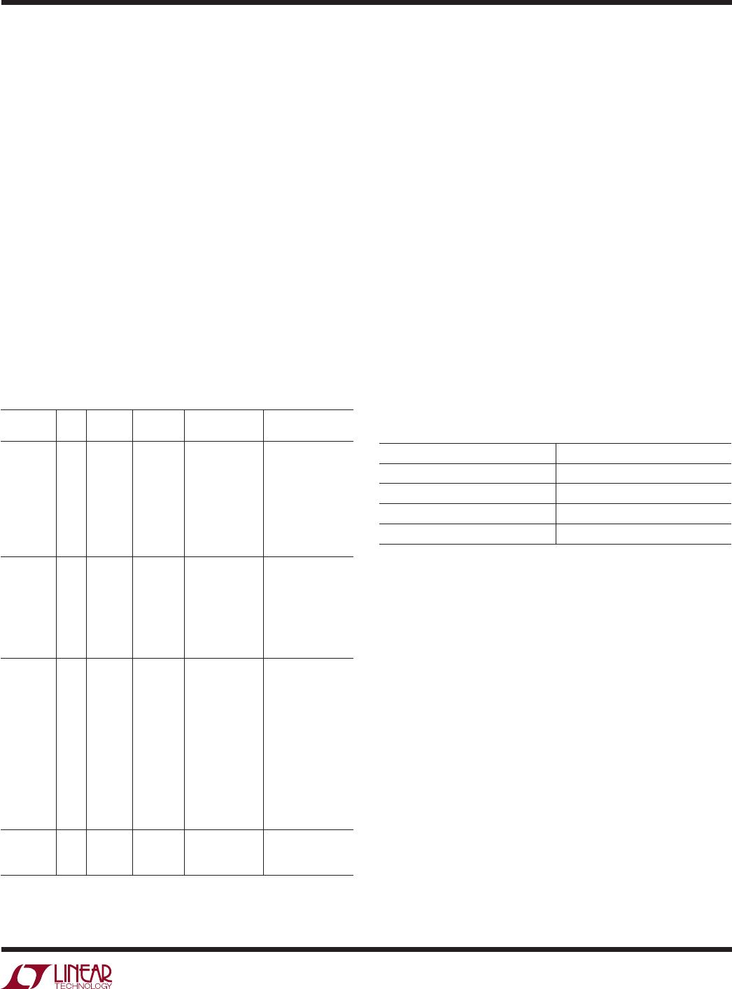
by application. Some inductors that may be suitable for
this application are listed in Table 6.
Table 6. Recommended Inductors
INDUCTOR
TYPE
L
(µH)
MAX
I
DC
(A)
MAX
DCR
(Ω)
SIZE in mm
(L × W × H)
MANUFACTURER
LPS4018
3.3 2.2 0.08 3.9 × 3.9 × 1.7 Coilcraft
www.coilcraft.com
D53LC
DB318C
3.3
3.3
2.26
1.55
0.034
0.070
5 × 5 × 3
3.8 × 3.8 × 1.8
Toko
www.toko.com
WE-TPC
Type M1
3.3 1.95 0.065 4.8 × 4.8 × 1.8 Wurth Elektronik
www.we-online.com
CDRH6D12
CDRH6D38
3.3
3.3
2.2
3.5
0.0625
0.020
6.7 × 6.7 × 1.5
7 × 7 × 4
Sumida
www.sumida.com
V
BUS
and V
OUT
Bypass Capacitors
The style and value of capacitors used with the LTC3555
family determine several important parameters such as
regulator control-loop stability and input voltage ripple.
Because the LTC3555 family uses a step-down switching
power supply from V
BUS
to V
OUT
, its input current wave-
form contains high frequency components. It is strongly
recommended that a low equivalent series resistance (ESR)
multilayer ceramic capacitor be used to bypass V
BUS
.
Tantalum and aluminum capacitors are not recommended
because of their high ESR. The value of the capacitor on
V
BUS
directly controls the amount of input ripple for a
given load current. Increasing the size of this capacitor
will reduce the input ripple.
To prevent large V
OUT
voltage steps during transient load
conditions, it is also recommended that a ceramic capaci-
tor be used to bypass V
OUT
. The output capacitor is used
in the compensation of the switching regulator. At least
4μF of actual capacitance with low ESR are required on
V
OUT
. Additional capacitance will improve load transient
performance and stability.
Multilayer ceramic chip capacitors typically have excep-
tional ESR performance. MLCCs combined with a tight
board layout and an unbroken ground plane will yield very
good performance and low EMI emissions.
There are several types of ceramic capacitors available,
each having considerably different characteristics. For
example, X7R ceramic capacitors have the best voltage and
temperature stability. X5R ceramic capacitors have appar-
ently higher packing density but poorer performance over
their rated voltage and temperature ranges. Y5V ceramic
capacitors have the highest packing density, but must be
used with caution because of their extreme non-linear
characteristic of capacitance verse voltage. The actual
in-circuit capacitance of a ceramic capacitor should be
measured with a small AC signal as is expected in-circuit.
Many vendors specify the capacitance versus voltage with
a 1V
RMS
AC test signal and as a result, overstate the ca-
pacitance that the capacitor will present in the application.
Using similar operating conditions as the application, the
user must measure or request from the vendor the actual
capacitance to determine if the selected capacitor meets
the minimum capacitance that the application requires.
General Purpose Switching Regulator Inductor
Selection
Many different sizes and shapes of inductors are avail-
able from numerous manufacturers. Choosing the right
inductor from such a large selection of devices can be
overwhelming, but following a few basic guidelines will
make the selection process much simpler.
The general purpose step-down converters are designed
to work with inductors in the range of 2.2µH to 10µH. For
most applications a 4.7µH inductor is suggested for the
lower power switching regulators 1 and 2 and 2.2µH is
recommended for the more powerful switching regula-
tor 3. Larger value inductors reduce ripple current which
improves output ripple voltage. Lower value inductors result
in higher ripple current and improved transient response
time. To maximize efficiency, choose an inductor with a
low DC resistance. For a 1.2V output, efficiency is reduced
about 2% for 100mΩ series resistance at 400mA load cur-
rent, and about 2% for 300mΩ series resistance at 100mA
load current. Choose an inductor with a DC current rating
at least 1.5 times larger than the maximum load current to
ensure that the inductor does not saturate during normal
operation. If output short circuit is a possible condition,
the inductor should be rated to handle the maximum peak
current specified for the step-down converters.
Different core materials and shapes will change the size/
current and price/current relationship of an inductor. Toroid
or shielded pot cores in ferrite or Permalloy materials are
small and dont radiate much energy, but generally cost
more than powdered iron core inductors with similar
APPLICATIONS INFORMATION
LTC3555/LTC3555-X
27
3555fe
For more information www.linear.com/LTC3555
electrical characteristics. Inductors that are very thin or
have a very small volume typically have much higher core
and DCR losses, and will not give the best efficiency. The
choice of which style inductor to use often depends more
on the price vs size, performance and any radiated EMI
requirements than on what the LTC3555 family requires
to operate.
The inductor value also has an effect on forced Burst
Mode and Burst Mode operations. Lower inductor values
will cause the Burst and forced Burst Mode switching
frequencies to increase.
Table 7 shows several inductors that work well with the
LTC3555 familys general purpose regulators. These in-
ductors offer a good compromise in current rating, DCR
and physical size. Consult each manufacturer for detailed
information on their entire selection of inductors.
Table 7. Recommended Inductors
INDUCTOR
TYPE
L
(µH)
MAX
I
DC
(A)
MAX
DCR (Ω)
SIZE in mm
(L × W × H)
MANUFACTURER
DE2818C
D312C
DE2812C
4.7
3.3
4.7
3.3
2.2
4.7
3.3
2.0
1.25
1.45
0.79
0.90
1.14
1.2
1.4
1.8
0.072
0.053
0.24
0.20
0.14
0.13*
0.10*
0.067*
3.0 × 2.8 × 1.8
3.0 × 2.8 × 1.8
3.6 × 3.6 × 1.2
3.6 × 3.6 × 1.2
3.6 × 3.6 × 1.2
3.0 × 2.8 × 1.2
3.0 × 2.8 × 1.2
3.0 × 2.8 × 1.2
Toko
www.toko.com
CDRH3D16
CDRH2D11
CLS4D09
4.7
3.3
2.2
4.7
3.3
2.2
4.7
0.9
1.1
1.2
0.5
0.6
0.78
0.75
0.11
0.085
0.072
0.17
0.123
0.098
0.19
4 × 4 × 1.8
4 × 4 × 1.8
4 × 4 × 1.8
3.2 × 3.2 × 1.2
3.2 × 3.2 × 1.2
3.2 × 3.2 × 1.2
4.9 × 4.9 × 1
Sumida
www.sumida.
com
SD3118
SD3112
SD12
SD10
4.7
3.3
2.2
4.7
3.3
2.2
4.7
3.3
2.2
4.7
3.3
2.2
1.3
1.59
2.0
0.8
0.97
1.12
1.29
1.42
1.80
1.08
1.31
1.65
0.162
0.113
0.074
0.246
0.165
0.14
0.117*
0.104*
0.075*
0.153*
0.108*
0.091*
3.1 × 3.1 × 1.8
3.1 × 3.1 × 1.8
3.1 × 3.1 × 1.8
3.1 × 3.1 × 1.2
3.1 × 3.1 × 1.2
3.1 × 3.1 × 1.2
5.2 × 5.2 × 1.2
5.2 × 5.2 × 1.2
5.2 × 5.2 × 1.2
5.2 × 5.2 × 1.0
5.2 × 5.2 × 1.0
5.2 × 5.2 × 1.0
Cooper
www.cooperet.
com
LPS3015 4.7
3.3
2.2
1.1
1.3
1.5
0.2
0.13
0.11
3.0 × 3.0
× 1.5
3.0 × 3.0 × 1.5
3.0 × 3.0 × 1.5
Coil Craft
www.coilcraft.
com
*Typical DCR
General Purpose Switching Regulator Input/Output
Capacitor Selection
Low ESR (equivalent series resistance) MLCC capacitors
should be used at both switching regulator outputs as well
as at each switching regulator input supply (V
INX
). Only X5R
or X7R ceramic capacitors should be used because they
retain their capacitance over wider voltage and temperature
ranges than other ceramic types. A 10μF output capaci-
tor is sufficient for most applications. For good transient
response and stability the output capacitor should retain
at least 4μF of capacitance over operating temperature
and bias voltage. Each switching regulator input supply
should be bypassed with a 1μF capacitor. Consult with
capacitor manufacturers for detailed information on their
selection and specifications of ceramic capacitors. Many
manufacturers now offer very thin (<1mm tall) ceramic
capacitors ideal for use in height-restricted designs. Table
8 shows a list of several ceramic capacitor manufacturers.
Table 8. Recommended Ceramic Capacitor Manufacturers
AVX www.avxcorp.com
Murata www.murata.com
Taiyo Yuden www.t-yuden.com
Vishay Siliconix www.vishay.com
TDK www.tdk.com
Over-Programming the Battery Charger
The USB high power specification allows for up to 2.5W to
be drawn from the USB port (5V × 500mA). The PowerPath
switching regulator transforms the voltage at V
BUS
to just
above the voltage at BAT with high efficiency, while limiting
power to less than the amount programmed at CLPROG.
In some cases the battery charger may be programmed
(with the PROG pin) to deliver the maximum safe charging
current without regard to the USB specifications. If there
is insufficient current available to charge the battery at the
programmed rate, the PowerPath regulator will reduce
charge current until the system load on V
OUT
is satisfied
and the V
BUS
current limit is satisfied. Programming the
battery charger for more current than is available will not
cause the average input current limit to be violated. It will
merely allow the battery charger to make use of all available
power to charge the battery as quickly as possible, and
with minimal power dissipation within the battery charger.
APPLICATIONS INFORMATION

LTC3555IUFD#TRPBF

Mfr. #:
Manufacturer:
Analog Devices / Linear Technology
Description:
Battery Management Hi Eff USB Pwr Manager + 3x Buck DC/DC
Lifecycle:
New from this manufacturer.
Delivery:
DHL FedEx Ups TNT EMS
Payment:
T/T Paypal Visa MoneyGram Western Union