LTC3555/LTC3555-X
22
3555fe
For more information www.linear.com/LTC3555
the LTC3555 family will remember the last input of valid
data that it received. Once all chips on the bus have been
addressed and sent valid data, a global STOP condition can
be sent and the LTC3555 family will update its command
latch with the data that it had received.
In certain circumstances the data on the I
2
C bus may
become corrupted. In these cases the LTC3555 family
responds appropriately by preserving only the last set of
complete data that it has received. For example, assume
the LTC3555 family has been successfully addressed and is
receiving data when a STOP condition mistakenly occurs.
The LTC3555 family will ignore this STOP condition and
will not respond until a new START condition, correct ad-
dress, new set of data and STOP condition are transmitted.
Likewise, with only one exception, if the LTC3555 family was
previously addressed and sent valid data but not updated
with a STOP, it will respond to any STOP that appears on
the bus, independent of the number of REPEAT-STARTS
that have occurred. If a REPEAT-START is given and the
LTC3555 family successfully acknowledges its address and
first byte, it will not respond to a STOP until both bytes
of the new data have been received and acknowledged.
Disabling the I
2
C Port
The I
2
C serial port can be disabled by grounding the DV
CC
pin. In this mode, control automatically passes to the in-
dividual logic input pins EN1, EN2, EN3, I
LIM0
, I
LIM1
, SDA
and SCL. Some functionality is not available in this mode
such as the programmability of switching regulators 2
and 3s output voltage and the battery charger disable
feature. In this mode, both of the programmable switching
regulators have a fixed servo voltage of 0.8V.
Because the SDA and SCL pins have no other context when
DV
CC
is grounded, these pins are re-mapped to control
the switching regulator mode bits B5 and B6. SCL maps
to B5 and SDA maps to B6.
RST3 Pin
The RST3 pin is an open-drain output used to indicate that
switching regulator 3 has reached its final voltage. RST3
remains low impedance until regulator 3 reaches 92% of
its regulation value. A 230ms delay is included to allow a
system microcontroller ample time to reset itself. RST3
may be used as a power-on reset to the microprocessor
powered by regulator 3 or may be used to enable regulators
1 and/or 2 for supply sequencing. RST3 is an open-drain
output and requires a pull-up resistor to the output volt-
age of regulator 3 or another appropriate power source.
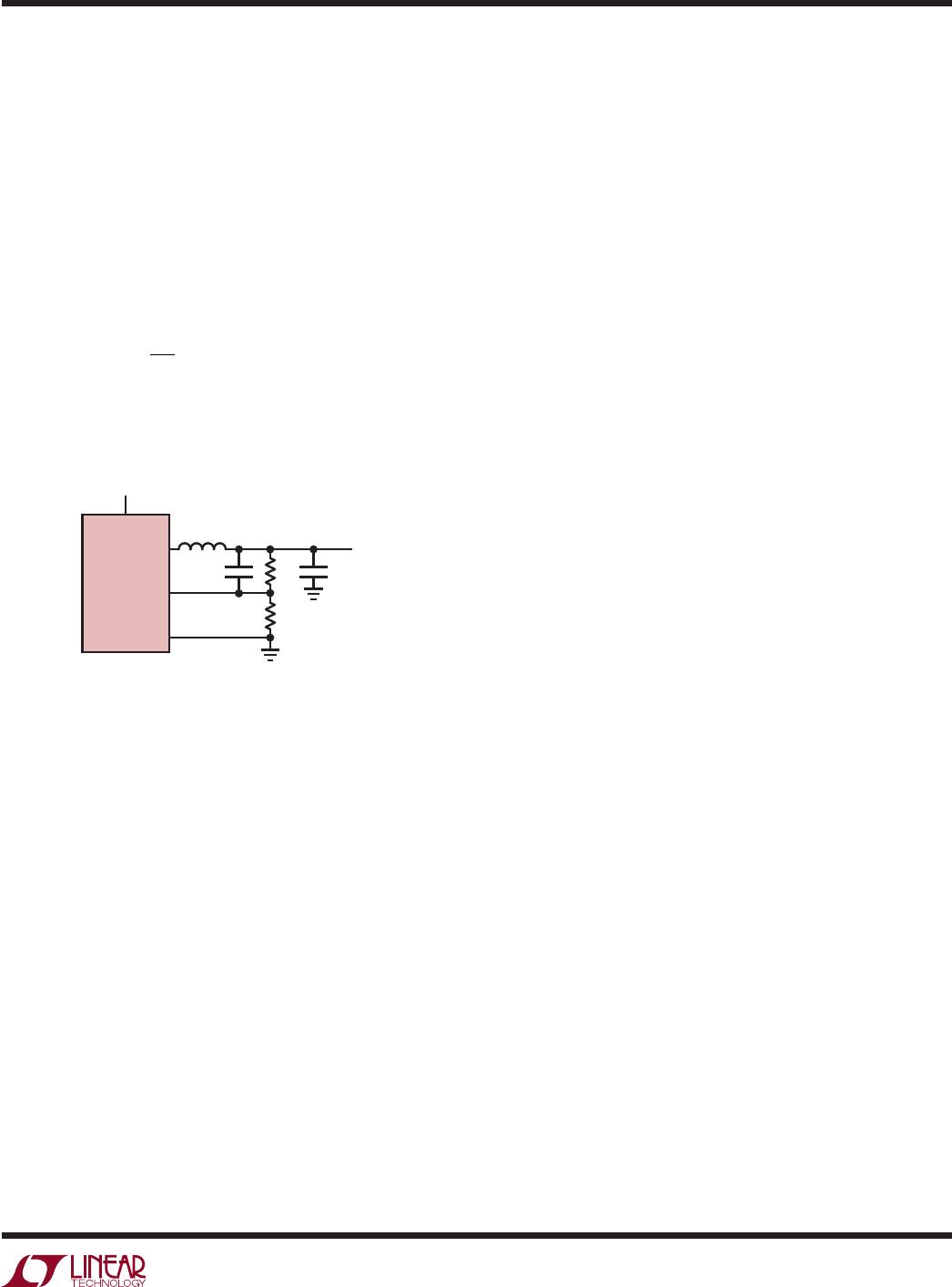
General Purpose Step-Down Switching Regulators
The LTC3555 family contains three general purpose
2.25MHz step-down constant-frequency current mode
switching regulators. Two regulators provide up to 400mA
and a third switching regulator can produce up to 1A.
All three switching regulators can be programmed for a
minimum output voltage of 0.8V and can be used to power
a microcontroller core, microcontroller I/O, memory, disk
drive or other logic circuitry. Two of the switching regulators
have I
2
C programmable set-points for on-the-fly power
savings. All three converters support 100% duty cycle
operation (low dropout mode) when their input voltage
drops very close to their output voltage. To suit a variety
of applications, selectable mode functions can be used
to trade-off noise for efficiency. Four modes are available
to control the operation of the LTC3555 familys general
purpose switching regulators. At moderate to heavy loads,
the pulse skip mode provides the least noise switching
solution. At lighter loads, either Burst Mode operation,
forced Burst Mode operation or LDO mode may be selected.
The switching regulators include soft-start to limit inrush
current when powering on, short-circuit current protection
and switch node slew limiting circuitry to reduce radiated
EMI. No external compensation components are required.
The operating mode of the regulators may be set by either
I
2
C control or by manual control of the SDA and SCL pins
if the I
2
C port is not used. Each converter may be individu-
ally enabled by either their external control pins EN1, EN2,
EN3 or by the I
2
C port. Switching regulators 2 and 3 have
individual programmable feedback servo voltages via I
2
C
control. The switching regulator input supplies V
IN1
, V
IN2
and V
IN3
will generally be connected to the system load
pin V
OUT
.
OPERATION
LTC3555/LTC3555-X
23
3555fe
For more information www.linear.com/LTC3555
Step-Down Switching Regulator Output Voltage
Programming
All three switching regulators can be programmed for
output voltages greater than 0.8V. Switching regulators 2
and 3 have I
2
C programmable set-points while regulator 1
has a single fixed set-point. The full-scale output voltage for
each switching regulator is programmed using a resistor
divider from the switching regulator output connected to
the feedback pins (FB1, FB2 and FB3) such that:
V
OUTX
= V
FBX
R1
R2
+ 1
where V
FBX
ranges from 0.425V to 0.8V for switching
regulators 2 and 3 and V
FBX
is fixed at 0.8V for switching
regulator 1. See Figure 4
latch which causes the main P-channel MOSFET switch to
turn off and the N-channel MOSFET synchronous rectifier
to turn on. The N-channel MOSFET synchronous rectifier
turns off at the end of the 2.25MHz cycle or if the current
through the N-channel MOSFET synchronous rectifier
drops to zero. Using this method of operation, the error
amplifier adjusts the peak inductor current to deliver the
required output power. All necessary compensation is
internal to the switching regulator requiring only a single
ceramic output capacitor for stability. At light loads in PWM
mode, the inductor current may reach zero on each pulse
which will turn off the N-channel MOSFET synchronous
rectifier. In this case, the switch node (SW) goes high
impedance and the switch node voltage will “ring”. This
is discontinuous mode operation, and is normal behavior
for a switching regulator. At very light loads in pulse skip
mode, the switching regulators will automatically skip
pulses as needed to maintain output regulation.
At high duty cycles (V
OUTx
> V
INx
/2) it is possible for the
inductor current to reverse, causing the regulator to operate
continuously at light loads. This is normal and regulation is
maintained, but the supply current will increase to several
milliamperes due to continuous switching.
In forced Burst Mode operation, the switching regulators
use a constant current algorithm to control the inductor
current. By controlling the inductor current directly and
using a hysteretic control loop, both noise and switching
losses are minimized. In this mode output power is limited.
While in forced Burst Mode operation, the output capacitor
is charged to a voltage slightly higher than the regulation
point. The step-down converter then goes into sleep mode,
during which the output capacitor provides the load cur-
rent. In sleep mode, most of the regulators circuitry is
powered down, helping conserve battery power. When the
output voltage drops below a pre-determined value, the
switching regulator circuitry is powered on and another
burst cycle begins. The duration for which the regulator
operates in sleep mode depends on the load current. The
sleep time decreases as the load current increases. The
maximum output current in forced Burst Mode operation is
about 100mA for switching regulators 1 and 2, and about
250mA for switching regulator 3. The step-down switching
regulators will not enter sleep mode if the maximum output
current is exceeded in forced Burst Mode operation and
OPERATION
Figure 4. Buck Converter Application Circuit
Typical values for R1 are in the range of 40k to 1M. The
capacitor C
FB
cancels the pole created by feedback resis-
tors and the input capacitance of the FB pin and also helps
to improve transient response for output voltages much
greater than 0.8V. A variety of capacitor sizes can be used
for C
FB
but a value of 10pF is recommended for most ap-
plications. Experimentation with capacitor sizes between
2pF and 22pF may yield improved transient response.
Step-Down Switching Regulator Operating Modes
The LTC3555 familys general purpose switching regulators
include four possible operating modes to meet the noise/
power needs of a variety of applications.
In pulse skip mode, an internal latch is set at the start of
every cycle which turns on the main P-channel MOSFET
switch. During each cycle, a current comparator compares
the peak inductor current to the output of an error amplifier.
The output of the current comparator resets the internal
V
INx
LTC3555/
LTC3555-X
L
SWx
R1 C
OUT
C
FB
V
OUTx
R2
3555 F04
FBx
GND
LTC3555/LTC3555-X
24
3555fe
For more information www.linear.com/LTC3555
OPERATION
the switching regulator input supply leaving only a few
nanoamperes of leakage current. The step-down switch-
ing regulator outputs are individually pulled to ground
through a 10k resistor on the switch pins (SW1-SW3)
when in shutdown.
General Purpose Switching Regulator Dropout
Operation
It is possible for a switching regulators input voltage,
V
INx
, to approach its programmed output voltage (e.g., a
battery voltage of 3.4V with a programmed output voltage
of 3.3V). When this happens, the PMOS switch duty cycle
increases until it is turned on continuously at 100%. In this
dropout condition, the respective output voltage equals the
regulator’s input voltage minus the voltage drops across
the internal P-channel MOSFET and the inductor.
Step-Down Switching Regulator Soft-Start Operation
Soft-start is accomplished by gradually increasing the
peak inductor current for each switching regulator over
a 500μs period. This allows each output to rise slowly,
helping minimize the battery surge current. A soft-start
cycle occurs whenever a given switching regulator is
enabled, or after a fault condition has occurred (thermal
shutdown or UVLO). A soft-start cycle is not triggered by
changing operating modes. This allows seamless output
operation when transitioning between forced Burst Mode,
Burst Mode, pulse skip mode or LDO operation.
Step-Down Switching Regulator Switching Slew Rate
Control
The step-down switching regulators contain new patent
pending circuitry to limit the slew rate of the switch nodes
(SWx). This new circuitry is designed to transition the
switch nodes over a period of a couple of nanoseconds,
significantly reducing radiated EMI and conducted supply
noise.
Low Supply Operation
The LTC3555 family incorporates an undervoltage lockout
circuit on V
OUT
which shuts down the general purpose
switching regulators when V
OUT
drops below V
OUTUVLO
.
This UVLO prevents unstable operation.
the output will drop out of regulation. Forced Burst Mode
operation provides a significant improvement in efficiency
at light loads at the expense of higher output ripple when
compared to pulse skip mode. For many noise-sensitive
systems, forced Burst Mode operation might be undesirable
at certain times (i.e., during a transmit or receive cycle
of a wireless device), but highly desirable at others (i.e.,
when the device is in low power standby mode). The I
2
C
port can be used to enable or disable forced Burst Mode
operation at any time, offering both low noise and low
power operation when they are needed.
In Burst Mode operation, the switching regulator automati-
cally switches between fixed frequency PWM operation and
hysteretic control as a function of the load current. At light
loads, the regulators operate in hysteretic mode in much
the same way as described for the forced Burst Mode
operation. Burst Mode operation provides slightly less
output ripple at the expense of slightly lower efficiency than
forced Burst Mode operation. At heavy loads the switch-
ing regulator operates in the same manner as pulse skip
operation at high loads. For applications that can tolerate
some output ripple at low output currents, Burst Mode
operation provides better efficiency than pulse skip at light
loads while still providing the full specified output current
of the switching regulator.
Finally, the switching regulators have an LDO mode that
gives a DC option for regulating their output voltages. In
LDO mode, the switching regulators are converted to linear
regulators and deliver continuous power from their SWx
pins through their respective inductors. This mode gives
the lowest possible output noise as well as low quiescent
current at light loads.
The step-down switching regulators allow mode transition
on the fly, providing seamless transition between modes
even under load. This allows the user to switch back and
forth between modes to reduce output ripple or increase
low current efficiency as needed.
Step-Down Switching Regulator in Shutdown
The step-down switching regulators are in shutdown when
not enabled for operation. In shutdown, all circuitry in
the step-down switching regulator is disconnected from

LTC3555IUFD#TRPBF

Mfr. #:
Manufacturer:
Analog Devices / Linear Technology
Description:
Battery Management Hi Eff USB Pwr Manager + 3x Buck DC/DC
Lifecycle:
New from this manufacturer.
Delivery:
DHL FedEx Ups TNT EMS
Payment:
T/T Paypal Visa MoneyGram Western Union